
Page 40 - Power Electronics Handbook
P. 40
Unipolar transistors 33
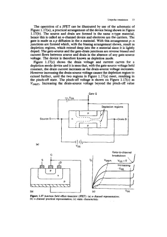
The operation of a JFET can be illustrated by use of the schematic of
Figure 1.17(a), a practical arrangement of the device being shown in Figure
l.l7(b). The source and drain are formed in the same n-type material,
hence this is called an n-channel device and electrons are the carriers. The
gate is made as a p diffusion in the n material. With this arrangement p-n
junctions are formed which, with the biasing arrangement shown, result in
depletion regions, which extend deep into the n material since it is lightly
doped. The gate-source and the gate-drain junctions are reverse biased and
current flows between source and drain in the absence of any gate-source
voltage. The device is therefore known as depletion mode.
Figure 1.17(c) shows the drain voltage and current curves for a
depletion-mode device and it is seen that, with the gate-source voltage held
constant, the drain current increases as the drain-source voltage increases.
However increasing the drain-source voltage causes the depletion region to
extend further, until the two regions in Figure 1.17(a) meet, resulting in
the pinch-off state. The pinch-off voltage is shown on Figure 1.17(c) as
VDs(p). Increasing the drain-source voltage beyond the pinch-off value
,,
I
4t
Depletion regions
I
I P
I '-- _---_
Source S A - , n : Drain D
------*
I
I P
I I
Gate-to-channel
G I breakdown /
S I
P
\\\\\\\\\\
Figure 1.17 Junction field effect transistor (JFET): (a) n-channel representation;
(b) n-channel practical representation; (c) static characteristic