
Page 36 - Power Electronics Handbook
P. 36
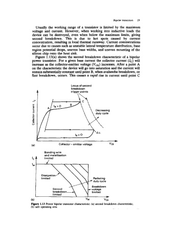
Bipolar transistors   29
                      Usually the working range of  a transistor is limited by  the maximum
                    voltage  and  current.  However,  when  working into  inductive loads the
                    device can be  destroyed,  even when  below the maximum limits,  giving
                    second  breakdown.  This  is  due  to  hot  spots  caused  by  current
                    concentration, resulting in local thermal runaway. Current concentrations
                    occur due to causes such as unstable lateral temperature distribution, base
                    region potential drops, uneven base widths, and uneven mounting of  the
                    silicon chip onto the heat sink.
                      Figure 1.13(a) shows the second breakdown characteristic of  a bipolar
                    power transistor.  For a given base current the collector current (I,)  will
                    increase as the collector-emitter voltage (V,)   increases. After a point A
                    on the characteristic the device will go into saturation and the current will
                    remain substantially constant until point B, when avalanche breakdown, or
                    first breakdown, occurs. This causes a rapid rise in current until point C


                                           Locus of second
                                           breakdown
                                           trigger points

                     ,.


                                                                     -
                                    Collector - emitter voltage   VCE
                    (a)
                            Bonding wire
                            and metallisation
                    IC f   limited
                              /


                                                        Reducing
                                                        duty cycle


                   (b)                              VM         "CE
                   Figure 1.13 Power bipolar transistor characteristic: (a) second breakdown characteristic;
                   (b) safe operating area