
Page 34 - Power Electronics Handbook
P. 34
Bipolar transistors 27
level, given by the collector-emitter sustaining voltage, the junction breaks
down, and the voltage across the transistor remains relatively constant,
until the energy in the inductor has been dissipated.
Figure l.ll(e) shows the transfer characteristic of a bipolar transistor.
With no base current the collector current equals the leakage value, given
by ZCEO. This leakage current decreases as the transistor is driven by
negative base current until it reaches a minimum value given by ZCBO,
known as the collector-base leakage current with no emitter current. It is
related to the collector-emitter leakage by equation (1.8).
ICE0 .= kB0 (l + hFE) (1.8)
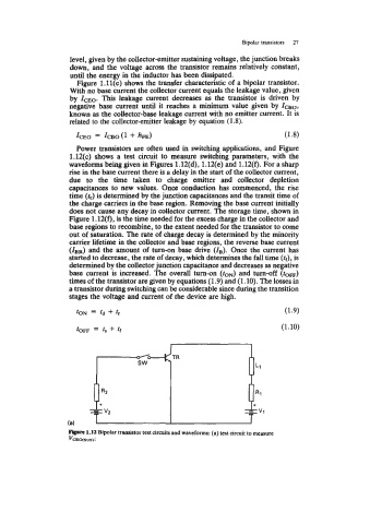
Power transistors are often used in switching applications, and Figure
1.12(c) shows a test circuit to measure switching parameters, with the
waveforms being given in Figures 1.12(d), 1.12(e) and 1.12(f). For a sharp
rise in the base current there is a delay in the start of the collector current,
due to the time taken to charge emitter and collector depletion
capacitances to new values. Once conduction has commenced, the rise
time (4) is determined by the junction capacitances and the transit time of
the charge carriers in the base region. Removing the base current initially
does not cause any decay in collector current. The storage time, shown in
Figure 1.12(f), is the time needed for the excess charge in the collector and
base regions to recombine, to the extent needed for the transistor to come
out of saturation. The rate of charge decay is determined by the minority
carrier lifetime in the collector and base regions, the reverse base current
(ZBR) and the amount of turn-on base drive (IB). Once the current has
started to decrease, the rate of decay, which determines the fall time (tf), is
determined by the collector junction capacitance and decreases as negative
base current is increased. The overall turn-on (roN) and turn-off (tom)
times of the transistor are given by equations (1.9) and (1.10). The losses in
a transistor during switching can be considerable since during the transition
stages the voltage and current of the device are high.
f0N = fd + tr (1.9)
ton: = t, + tf (1.10)
(a)
pirvc 1.12 Bipolar transistor test circuits and waveforms: (a) test circuit to measure
vcEocsus,;