
Page 41 - Power Electronics Handbook
P. 41
34 Power semiconductor devices
does not cause any significant increase in drain current, but the point along
the channel at which the depletion regions meet moves nearer to the
source. The drain current is maintained by the electrons being swept
through the depletion layer, similar to the process in the base of a bipolar
transistor. Eventually the breakdown region is reached at high values of
voltage. Making the gate-source voltage negative lowers the value of
drain-source voltage at which pinch-off occurs.
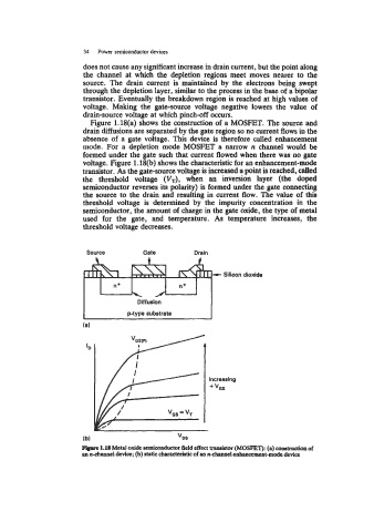
Figure 1.18(a) shows the construction of a MOSFET. The source and
drain diffusions are separated by the gate region so no current flows in the
absence of a gate voltage. This device is therefore called enhancement
mode. For a depletion mode MOSET a narrow n channel would be
formed under the gate such that current flowed when there was no gate
voltage. Figure 1.18(b) shows the characteristic for an enhancement-mode
transistor. As the gate-source voltage is increased a point is reached, called
the threshold voltage (VT), when an inversion layer (the doped
semiconductor reverses its polarity) is formed under the gate connecting
the source to the drain and resulting in current flow. The value of this
threshold voltage is determined by the impurity concentration in the
semiconductor, the amount of charge in the gate oxide, the type of metal
used for the gate, and temperature. As temperature increases, the
threshold voltage decreases.
Source Gate Drain
Silicon dioxide
D-tvDe substrate
(a J
'D
Increasing
-t "GS
Figure 1.18 Metal oxide scmioonductor field effect transistor (MOSFET): (a) comtruction of
an n-chaanel device; (b) static characteristic of an n-chmncl enhancement-mode device