
Page 46 - Power Electronics Handbook
P. 46
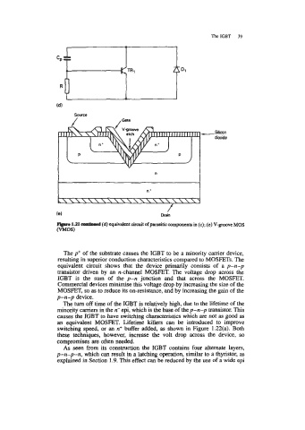
TheIGBT   39


                                                                      -Silicon
                                                                          dioxide


                       The p+ of the substrate causes the IGBT to be a minority carrier device,
                     resulting in superior conduction characteristics compared to MOSFETs. The
                     equivalent circuit  shows  that  the  device  primarily  consists of  a p-n-p
                     transistor driven by  an n-channel MOSFET. The voltage drop across the
                     IGBT  is  the  sum  of  the  p-n  junction  and  that  across  the  MOSFET.
                     Commercial devices minimise this voltage drop by increasing the size of the
                     MOSFET, so as to reduce its on-resistance, and by increasing the gain of the
                     p-n-p  device.
                       The turn off time of the IGBT is relatively high, due to the lifetime of the
                     minority carriers in the n- epi, which is the base of the p-n-p  transistor. This
                     causes the IGBT to have switching characteristics which are not as good as
                     an equivalent MOSFET.  Lifetime  killers  can  be  introduced  to  improve
                     switching speed, or an n+ buffer added, as shown in Figure  1.22(a). Both
                     these  techniques,  however, increase the  volt  drop  across the  device,  so
                     compromises are often needed.
                       As  seen from its construction the  IGBT contains four alternate layers,
                     p-n-p-n,   which can result in a latching operation, similar to a thyristor, as
                     explained in Section 1.9. This effect can be reduced by the use of a wide epi