
Page 49 - Power Electronics Handbook
P. 49
42 Power semiconductor devices
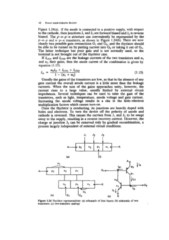
Figure 1.24(a). If the anode is connected to a positive supply, with respect
to the cathode, then junctions J1 and J3 are forward biased and J2 is reverse
biased. The p-n-p-n structure can conveniently be represented by the
p-n-p and n-p-n transistors, as shown in Figure 1.24(b). There are now
clearly two possible gate connections G1 and Gz, and the thyristor should
be able to be turned on by putting current into Gz or taking it out of GI.
The latter technique has poor gain and is not normally used, so the
terminal is not brought out of the thyristor case.
If Zcol and ZCo2 are the leakage currents of the two transistors and a1
and a2 their gains, then the anode current of the combination is given by
equation (1.15).
(1.15)
Usually the gains of the transistors are low, so that in the absence of any
gate current the overall anode current is a little more than the leakage
currents. When the sum of the gains approaches unity, however, the
current rises to a large value, usually limited by external circuit
impedances. Several techniques can be used to raise the gain of the
transistors, such as light, temperature, anode voltage and gate current.
Increasing the anode voltage results in a rise in the hole-electron
multiplication factors which causes turn-on.
Once the thyristor is conducting, its junctions are heavily doped with
holes and electrons. To turn the device off the polarity of anode and
cathode is reversed. This causes the carriers from J1 and J3 to be swept
away to the supply, resulting in a reverse recovery current. However, the
charge at junction J2 can be removed only by gradual recombination, a
process largely independent of external circuit conditions.
Jl J2 J3
Figure 1.24 Thyristor representations: (a) schematic of four layers; (b) schematic of two
transistors; (c) two-transistor analogy