
Page 56 - Power Electronics Handbook
P. 56
The gate turn-off switch 49
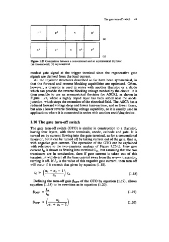
Figure 1.27 Comparison between a conventional and an asymmetrical thyristor:
(a) conventional; (b) asymmetrical
modest gate signal at the trigger terminal since the regenerative gate
signals are derived from the load current.
All the thyristor structures demibed so far have been symmetrical, in
that the forward and reverse blocking capabilities are optimised. Often,
however, a thyristor is used in series with another thyristor or a diode
which can provide the reverse blocking voltage needed by the circuit. It is
then possible to use an asymmetrical thyristor (or ASCR), as shown in
Figure 1.27, where a highly doped layer has been added near the anode
junction, which stops the extension of the electrical field. The ASCR has a
reduced forward voltage drop and lower turn-on time, and so lower losses,
but also a lower reverse blocking voltage capability, so it is usually used in
applications where it is connected in series with another rectifying device.
1.10 The gate turn-off switch
The gate turn-off switch (GTO) is similar in construction to a thyristor,
having four layers, with three terminals, anode, cathode and gate. It is
turned on by current flowing into the gate terminal, as for a conventional
thyristor, but it can be turned off by taking current out of the gate, that is,
with negative gate current. The operation of the GTO can be explained
with reference to the two-transistor analogy of Figure 1.25(c). Here gate
current ZG is shown as flowing into terminal G2, but assuming that the two
transistors are in conduction, then if gate current is taken out of this
terminal, it will divert all the base current away from the n-p-n transistor,
turning it off. If ZG is the value of this negative gate current, then turn-off
will occur if it exceeds that given by equation (1.18).
(1.18)
Defining the turn-off gain $om of the GTO by equation (1.19), allows
equation (1.18) to be rewritten as in equation (1.20).
BOFF = - (1.19)
IA
ZG