
Page 57 - Power Electronics Handbook
P. 57
50 Power semiconductor devices
A large value of turn-off gain for a GTO is desirable for an efficient
device. It can be increased by making the gain of the n-p-n transistor (a2)
as close to unity as possible, by having a narrow base region (pl) and heavily
doping the emitter (q). At the same time the gain of thep-n-p transistor (a,)
must be kept low, by making its base (n2) wide and adding gold doping, or
using some other lifetime control technique. These modifications give a fast
recovery device, but also result in the GTO having a higher voltage drop than
a thyristor.
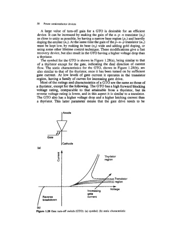
The symbol for the GTO is shown in Figure 1.28(a), being similar to that
of a thyristor except for the gate, indicating the dual direction of current
flow. The static characteristics for the GTO, shown in Figure 1.28(b), are
also similar to that of the thyristor, once it has been turned on by sufficient
gate current. At low levels of gate current it operates in the transistor
region, having a family of curves for increasing gate drive.
Most of the ratings and characteristics of a GTO are the same as those of
a thyristor, except for the following. The GTO has a high forward blocking
voltage rating, comparable to that attainable from a thyristor, but its
reverse voltage rating is lower, and in this aspect it is similar to a transistor.
The GTO also has a higher voltage drop and a higher latching current than
a thyristor. This latter parameter means that the gate drive needs to be
A/,,/
C Thyristor
Thyristor
region
region
-----
----- -- Transistor
region
region
/
’.
gate
current
Increasing
Voltage
Voltage
lncreasina - -- Transistor
gate
current
(b)
Figure 1.28 Gate turn-off switch (GTO): (a) symbol; (b) static characteristic