
Page 14 - Power Electronics Handbook
P. 14
Fabrication process 7
again avoided. Since in both the floating-zone and pedestal-pulling
methods the molten silicon is held in place by surface tension, the size of
the melt, and therefore of the silicon bars (and wafers) produced by these
methods, cannot be very large. These techniques are used for making
relatively low-power components.
During preparation of pure silicon, impurities of p or n type can be
added to the melt, to give the final silicon ingots the required resistivity.
The ingots are then cut into slices, using a diamond-impregnated saw. The
saw cuts are made along the <111> or <loo> planes of the crystal. These
cuts usually damage the crystal lattice near the silicon surface, resulting in
poor resistivity and minority carrier lifetime. The damaged area, which is
about 20pm deep, is removed by etching in a mixture of hydrofluoric and
nitric acids, and the surface is then polished to give a strain-free, highly flat
region.
1.2.2 oxide growth
Silicon oxide, also called silica or SiO,, may be grown and removed several
times from the suxface of the silicon slice during manufacture of the
semiconductor device. The oxide layer is used for diffusion masking, for
sealing and passivating the silicon surface, and for insulating the metal
intemnncctions from the silicon. Although the oxide layer may be
deposited onto the slice, as done for the epitaxy layer described in the next
section, it is more usual to grow it using dry or wet oxygen or steam.
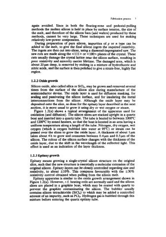
Figure 1.2(a) shows a typical arrangement of the apparatus used for
oxidation (and diffusion). The silicon slices are stacked upright in a quartz
boat and inserted into a quartz tube. The tube is heated to between 1ooo"C
and 1200°C by zoned heaters, so that the boat is located in an area having a
uniform temperature along a length of the tube. Nitrogen, dry oxygen, wet
oxygen (which is oxygen bubbled into water at 95OC) or steam can be
passed over the slices to grow the oxide layer. A thickness of about 1 pn
takes about 4 h to grow and consumes between 0.4 pn and 0.5 pm of the
silicon. The colour of the silicon surface changes with the thickness of the
oxide layer, due to the shift in the wavelength of the reflected light. This
effect is used as an indication of the layer thickness.
1.2.3 Epitaxy pwtb
Epitaxy means growing a single-crystal silicon structure on the original
slice, such that the new structure is essentially a molecular extension of the
original silicon. Epitaxy layers can be closely controlled regarding size and
resistivity, to about 210%. This compares favourably with the f30%
resistivity control obtained when pulling from the silicon melt.
Epitaxy apparatus is similar to the oxide growth arrangement shown in
Figure 1.2(a). However, r.f. heating coils are normally used and the silicon
slices are placed in a graphite boat, which may be coated with quartz to
prevent the graphite contaminating the silicon. The bubbler usually
contains silicon tetrachloride (Sit&) to which may be added a controlled
amount of an impurity, such as Pa3. Hydrogen gas is bubbled through this
mixture before entering the quartz epitaxy tube.