
Page 158 - Power Electronics Handbook
P. 158
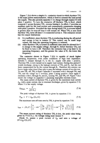
D.C. contacton   151
                     Figure 7.2(a) shows a simple d.c. contactor circuit in which thyristor TH1
                   is the main power semiconductor, which is fired to COM& the load across
                   the supply. This also permits capacitor C to charge through resistor R with
                   plate  1 positive. To turn the contactor off  thyristor TH2 is fired, which
                   connects C across thyristor THl, reverse biasing it. In effect, C provides an
                   auxiliary path for the load current and consequently commences charging
                   with plate 2 positive. Provided the time during which THl is reverse biased
                   is greater than its turn-off time it will remain off. When TH1 next fired
                                                                         is
                   thyristor TH2 turns off since C is connected across it. This contactor circuit
                   has two major limitations:

                   (i)  It is inefficient, since thyristor THz is conducting during the off period
                        and  energy is  lost  in  resistor R. This resistor can be made  large
                        valued, but then the operating frequency is reduced.
                   (ii)  After thyristor THl is turned on sufficient time must be allowed for C
                        to charge to the supply voltage, through R, before thyristor THz can
                        be fired to turn it off. Therefore the contactor has a top limit to its
                        operating frequency, and the greater the value of  R, the lower this
                        frequency.
                     The  contactor  shown  in  Figure  7.2(b)  is  capable  of  much  higher
                   operating  frequencies,  even  under  conditions  of  high  load  impedance.
                   Initially C  charges  through  D3 to  the  d.c.  supply  with  plate  1 positive.
                   Thyristor TH, is now turned on to supply load current. During this period C
                   would discharge, owing to the leakage currents of TH2 and D3, had this not
                   been compensated for by  the current through R1. Therefore this resistor can
                   have a large value since it has only to pass the leakage current of two devices.
                   To turn TH, off, TH, is fired. Capacitor C resonates with L through TH, and
                   TH,  and the volage on  C reverses, plate 2 being positive. Once again  C
                   resonates with L through D2 and D,,  turning TH, and TH, off. Figure 7.2(c)
                   shows the voltage on capacitor C assuming negligible resonant losses.
                     The mean current of thyristor TH, is given by the maximum load current
                   Ipk, with a peak current, due to resonant discharges, given by equation (7.4)
                   where V is the supply voltage.


                     The peak voltage of  thyristor TH, is given by  equation (7.5)

                     vpk  = v -k  lpk J(LI/c)                                  (7.5)
                                               ,/($)I
                    The maximum turn-off time seen by TH, is given by equation (7.6)
                   tom  =  J(L,C) [;  - sin-'  [$       + cos-' [:  ,/($-)]I   (7.6)


                     The mean current rating of  thyristor TH2 is low, the peak value being
                   given by VV(C/&).  Its voltage rating must exceed V.
                     Diode  Dl  passes  a  peak  current  of  Z,,k  and  sees a  voltage  of
                   2V+ZP~V(L1IC).