
Page 217 - Power Electronics Handbook
P. 217
The effect of source reactance 207
Phase voltages
Phase voltages
/--\
/
L-1
03 LD6,Dl-Dl ,Dl,D6 D3,D3,D3,04_ D5-05J
D6 04 D6 D6 D6 D2-)D6 D2 D4 D2 D4 D4
D4 04 D2 D2 D2 D2
Line voltage input p = 70"
cx (forced) = 40"
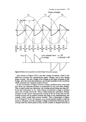
Flgare 9.32 Mode-three operation in a diode bridge with source reactance
Also shown in Figure 9.30 is one line voltage waveform, which is the
difference between the instantaneous phase voltages and is zero during
phase overlap. The line voltage is the voltage at the input terminals of the
bridge, after the series line inductors, and would normally be the waveform
which operated any internal control circuits.
In the waveforms of Figure 9.30 the overlap conditions have been such
that there are alternate periods of conduction by two and three diodes.
This is called mode-one operation, the overlap period being less than 60".
If the line inductance or d.c. load current is increased a stage is reached
where the overlap will be 60". This is called mode-two operation. Further
increase in load current will keep the overlap at 60" for some time but the
overlap period will be shifted towards the peak of the instantaneous line
voltage, which would help current transfer. This is illustrated in Figure
9.31. In Figure 9.31(a), for instance, at &,current should transfer to the top
diode in red phase, but the red phase voltage is held below this point due to
overlap with the yellow phase so that current transfer is delayed until this is