
Page 212 - Power Electronics Handbook
P. 212
The effect of source reactance 203
. tOl/ . 1,*
to
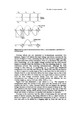
nrprC 9.26 Two-pulse bi-directional converter with a.c. source hpedance, operating in an
inversion mode
Overlap effects are not restricted to bidirectional converters. For
instance, Figure 9.27 shows the load voltage and device currents for the
circuit of Figure 9.15(a), assuming that the load current is ripple free and
the input lines have series reactances. Prior to to thyristors THz and TH3
were conducting. At to the supply voltage reverses and the load current
begins to transfer from the thyristors to the free-wheeling diode D1. Line
reactances prevent this occumng instantaneously, although the load
voltage is zero since D1 is conducting. At tol current has transferred
completely to D1 and TH2 and TH3 go off. When THI and TH, are fired at
rO2 there is again an overlap angle p2 due to the finite time for the current to
transfer from D, to the thyristors before the load voltage rises to that of the
supply, so that the effect of overlap has once again been to remove a portion
from the load voltage waveform during every half cycle. Since the
instantaneous line voltages at the overlap periods are different the two
overlap angles pl and c(2 will also differ, with p1 > p2.
Figure 9.27 has illustrated a case where cy > pl. The situation is
complicated when the revene is true, since now the current in D1 never
reaches the full d.c. value, because before this can happen the opposite
bridge thyristor is fired and the current will be caused to decay in D1. The
zero period in the load voltage waveform is equal to the sum of the two
overlap periods, during which partial current transfers from thyristor to
diode and diode to thyristor, in parallel with thyristor to thyristor.
Overlap in the converter has the effect of increasing the rise and fall
times of device currents, this being reflected to the a.c. input current, as
shown in Figure 9.28. The fundamental component of the a.c. current is
now also seen to be shifted by a lagging angle Q1 from the case for no