
Page 452 - Schaum's Outline of Theory and Problems of Applied Physics
P. 452
CHAP. 35] THE SOLID STATE 437
SOLVED PROBLEM 35.11
Explain the operation of a simple junction transistor.
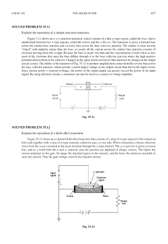
Figure 3-11 shows an n-p-n junction transistor, which consists of a thin p-type region, called the base, that is
sandwiched between two n-type regions, called the emitter and the collector. The transistor is given a forward bias
across the emitter-base junction and a reverse bias across the base-collector junction. The emitter is more heavily
“doped” with impurity atoms than the base, so nearly all the current across the emitter-base junction consists of
electrons moving from left to right. Because the base is made very thin and the concentration of holes there is low,
most of the electrons that enter the base diffuse through it to the base-collector junction where the high positive
potential attracts them to the collector. Changes in the input circuit current are thus mirrored by changes in the output
circuit current. The ability of the transistor of Fig. 35-11 to produce amplification comes from the reverse bias across
the base-collector junction, which permits a much higher voltage in the output circuit than that in the input circuit.
Since electric power = (current)(voltage), the power of the output signal can greatly exceed the power of the input
signal. By using different circuits, a transistor can also be used as a current or voltage amplifier.
Base
Emitter Collector
n p n
Input Output
signal load
− + − +
Fig. 35-11
SOLVED PROBLEM 35.12
Explain the operation of a field-effect transistor.
Figure 35-12 shows an n-channel field-effect transistor that consists of a strip of n-type material with contacts at
both ends together with a strip of p-type material, called the gate, on one side. When connected as shown, electrons
move from the source terminal to the drain terminal through the n-type channel. The p-n junction is given a reverse
bias, and as a result both the n and p materials near the junction are depleted of charge carriers. The higher the
reverse potential on the gate, the larger the depleted region in the channel, and the fewer the electrons available to
carry the current. Thus the gate voltage controls the channel current.
Fig. 35-12