Page 120 - Semiconductor For Micro- and Nanotechnology An Introduction For Engineers
P. 120
Free and Bound Electrons, Dimensionality Effects
                                ⁄
                             dψ dx
                                     must be fulfilled. This yields a system of four equations that
                                                                    ,
                                                                 ,
                                                                       ,
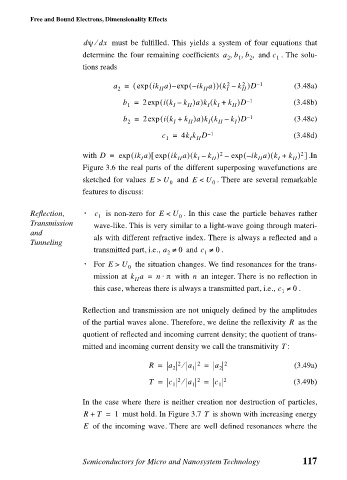
                             determine the four remaining coefficients  a b b  and c  . The solu-
                                                                 2  1  2     1
                             tions reads
                                                               (
                                                                 2
                                                                    2
                                                   –
                                    a =  ( exp ( ik a) exp  – (  ik a)) k –  k )D – 1  (3.48a)
                                                                    II
                                     2
                                                II
                                                           II
                                                                I
                                                 (
                                                            (
                                       b =  2exp ( ik –  k )a)k k +  k )D – 1    (3.48b)
                                        1          I   II   I  I  II
                                                 (
                                                             (
                                       b =  2exp ( ik +  k )a)k k –  k )D – 1    (3.48c)
                                                                  I
                                                              II
                                        2
                                                   I
                                                       II
                                                            I
                                                c =  4k k D – 1                  (3.48d)
                                                 1     I II
                                                                           (
                                                                                   2
                                                       (
                                                               2
                             with D =  exp ( ik a) exp[  ( ik a) k –  k ) –  exp (  i – k a) k +  k ) ]  .In
                                           I        II   I   II         II   I   II
                             Figure 3.6 the real parts of the different superposing wavefunctions are
                             sketched for values  E >  U   and  E <  U  . There are several remarkable
                                                  0          0
                             features to discuss:
                Reflection,   • c   is non-zero for  E <  U  . In this case the particle behaves rather
                                 1                   0
                Transmission   wave-like. This is very similar to a light-wave going through materi-
                and
                               als with different refractive index. There is always a reflected and a
                Tunneling
                               transmitted part, i.e., a ≠  0   and c ≠  . 0
                                                  2        1
                             • For  E >  U   the situation changes. We find resonances for the trans-
                                        0
                                                ⋅
                               mission at  k a =  n π   with   an integer. There is no reflection in
                                                        n
                                          II
                               this case, whereas there is always a transmitted part, i.e., c ≠  . 0
                                                                              1
                             Reflection and transmission are not uniquely defined by the amplitudes
                                                                                R
                             of the partial waves alone. Therefore, we define the reflexivity   as the
                             quotient of reflected and incoming current density; the quotient of trans-
                             mitted and incoming current density we call the transmitivity  :
                                                                              T
                                             R =  a 2  2  ⁄  a 1  2  =  a 2  2   (3.49a)
                                             T =  c  2  ⁄  a  2  =  c  2         (3.49b)
                                                   1    1     1
                             In the case where there is neither creation nor destruction of particles,
                             R +  T =  1   must hold. In Figure 3.7 T   is shown with increasing energy
                             E   of the incoming wave. There are well defined resonances where the
                             Semiconductors for Micro and Nanosystem Technology    117

