Page 189 - Semiconductor For Micro- and Nanotechnology An Introduction For Engineers
P. 189
Statistics
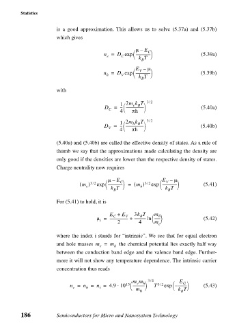
is a good approximation. This allows us to solve (5.37a) and (5.37b)
which gives
µ – E C
n = D exp ---------------- (5.39a)
k T
C
e
B
E – µ
V
n = D exp ---------------- (5.39b)
k T
h
V
B
with
/
1 2m k T 32
e B
D = --- ------------------- (5.40a)
C 4 πh
/
1 2m k T 32
h B
D = --- -------------------- (5.40b)
V 4 πh
(5.40a) and (5.40b) are called the effective density of states. As a rule of
thumb we say that the approximations made calculating the density are
only good if the densities are lower than the respective density of states.
Charge neutrality now requires
V
/
( m ) 32 exp µ – E C ( m ) 32 exp E – µ (5.41)
/
---------------- =
----------------
e k T h k T
B B
For (5.41) to hold, it is
E + E V 3k T m h
B
C
µ = -------------------- + -------------ln ------ (5.42)
i m
2 4 e
where the index i stands for “intrinsic”. We see that for equal electron
and hole masses m = m the chemical potential lies exactly half way
e h
between the conduction band edge and the valence band edge. Further-
more it will not show any temperature dependence. The intrinsic carrier
concentration thus reads
/
E
G
e
/
⋅
-------------
n = n = n = 4.9 10 15 m m h 34 T 32 exp – --------- (5.43)
m
i
e
h
B
0 k T
186 Semiconductors for Micro and Nanosystem Technology

