
Page 190 - Semiconductor For Micro- and Nanotechnology An Introduction For Engineers
P. 190
Electron Distribution Functions
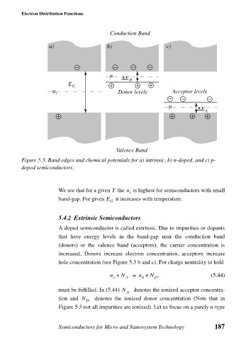
a) b) Conduction Band c)
µ
∆E D
E
G
µ i Donor levels Acceptor levels
µ
∆E A
Valence Band
Figure 5.3. Band edges and chemical potentials for a) intrinsic, b) n-doped, and c) p-
doped semiconductors.
T
We see that for a given the n i is highest for semiconductors with small
band-gap. For given E G it increases with temperature.
5.4.2 Extrinsic Semiconductors
A doped semiconductor is called extrinsic. Due to impurities or dopants
that have energy levels in the band-gap near the conduction band
(donors) or the valence band (acceptors), the carrier concentration is
increased. Donors increase electron concentration, acceptors increase
hole concentration (see Figure 5.3 b and c). For charge neutrality to hold
n + N A - = n + N D + (5.44)
e
h
must be fulfilled. In (5.44) N denotes the ionized acceptor concentra-
A -
tion and N denotes the ionized donor concentration (Note that in
D +
Figure 5.3 not all impurities are ionized). Let us focus on a purely n-type
Semiconductors for Micro and Nanosystem Technology 187