
Page 192 - Semiconductor For Micro- and Nanotechnology An Introduction For Engineers
P. 192
Electron Distribution Functions
N
E
G
D
C
----------
------------------exp
µ = E + k T ln ---------- 1 + 1 + 4D D V – k T (5.49)
C
B
2
2D C N D B
In the case of sufficiently low temperatures the ionized impurity concen-
tration plays the leading part and we assume n « N and thus write
h D +
n = N . This limiting case has a chemical potential of
D +
1 1 N ∆E D
D
µ = E + k T ln – --- + --- + -------exp ----------- (5.50)
D B k T
2 4 D C B
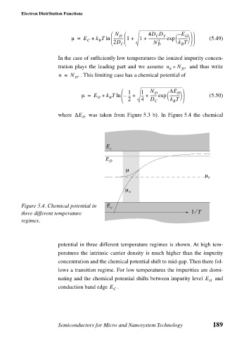
where ∆E D was taken from Figure 5.3 b). In Figure 5.4 the chemical
E
c
E
D
µ
µ
i
µ
o
Figure 5.4. Chemical potential in E v
⁄
three different temperature 1 T
regimes.
potential in three different temperature regimes is shown. At high tem-
peratures the intrinsic carrier density is much higher than the impurity
concentration and the chemical potential shift to mid-gap. Then there fol-
lows a transition regime. For low temperatures the impurities are domi-
nating and the chemical potential shifts between impurity level E and
D
conduction band edge E .
C
Semiconductors for Micro and Nanosystem Technology 189