
Page 23 - Semiconductor For Micro- and Nanotechnology An Introduction For Engineers
P. 23
Introduction
placed in a low-cost SMD package, is used in MAP and BAP tire pres-
sure applications. With an annual production running to several millions,
it is currently sold to leading automotive customers [1.2].
MEMS has to date spawned off two further terms that are of relevance to
us, namely MOEMS, for micro-opto-electro-mechanical systems, and
NEMS, for the inevitable nano-electro-mechanical systems.
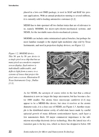
MOEMS can include entire miniaturized optical benches, but perhaps the
most familiar example is the digital light modulator chip sold by Texas
Instruments, and used in projection display devices, see Figure 1.2.
Figure 1.2. MOEMS device.
This 30 µm by 30 µm device is
a single pixel on a chip that has as
many pixels as a modern computer
screen display. Each mirror is
individually addressable, and
deflects light from a source to a
systems of lenses that project the
pixel onto a screen. Illustration ©
Texas Instruments Corp., Dallas
[1.3].
As for NEMS, the acronym of course refers to the fact that a critical
dimension is now no longer the large micrometer, but has become a fac-
tor 1000 smaller. The atomic force microscope cantilever [1.4] may
appear to be a MEMS-like device, but since it resolves at the atomic
diameter scale, it is a clear case of NEMS, see Figure 1.3. Another exam-
ple is the distributed mirror cavity of solid-state lasers made by careful
epitaxial growth of many different semiconductor layers, each layer a
few nanometers thick. Of major commercial importance is the sub-
micron microchip electronic device technology. Here the lateral size of a
transistor gate is the key size, which we know has dropped to below 100
22 Semiconductors for Micro and Nanosystem Technology