
Page 24 - Semiconductor For Micro- and Nanotechnology An Introduction For Engineers
P. 24
Popular Definitions and Acronyms
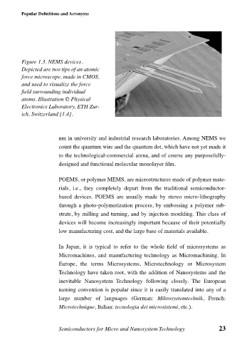
Figure 1.3. NEMS devices.
Depicted are two tips of an atomic
force microscope, made in CMOS,
and used to visualize the force
field surrounding individual
atoms. Illustration © Physical
Electronics Laboratory, ETH Zur-
ich, Switzerland [1.4].
nm in university and industrial research laboratories. Among NEMS we
count the quantum wire and the quantum dot, which have not yet made it
to the technological-commercial arena, and of course any purposefully-
designed and functional molecular monolayer film.
POEMS, or polymer MEMS, are microstructures made of polymer mate-
rials, i.e., they completely depart from the traditional semiconductor-
based devices. POEMS are usually made by stereo micro-lithography
through a photo-polymerization process, by embossing a polymer sub-
strate, by milling and turning, and by injection moulding. This class of
devices will become increasingly important because of their potentially
low manufacturing cost, and the large base of materials available.
In Japan, it is typical to refer to the whole field of microsystems as
Micromachines, and manufacturing technology as Micromachining. In
Europe, the terms Microsystems, Microtechnology or Microsystem
Technology have taken root, with the addition of Nanosystems and the
inevitable Nanosystem Technology following closely. The European
naming convention is popular since it is easily translated into any of a
large number of languages (German: Mikrosystemtechnik, French:
Microtechnique, Italian: tecnologia dei microsistemi, etc.).
Semiconductors for Micro and Nanosystem Technology 23