
Page 237 - Semiconductor For Micro- and Nanotechnology An Introduction For Engineers
P. 237
Interacting Subsystems
an offset in the measured magnetic field sensor that is more indicative of
packaging stress levels and the temperature—in this case the stress is
parasitic.
The chapter shows how interactions have successfully lead to innovative
semiconductor devices, and how the preceding analysis can help both to
understand the phenomena, as well as to extract design rules that help
create better device and system designs. Ultimately, in our view, engi-
neering theory is justified when it leads to better design methods. Of
course we cannot deal with all possibilities, and as a result we have made
a selection based on our own interests. We hope, however, that one con-
cept will remain more strongly than others: that it is the interaction or
coupling of natural “systems” that lead to useful (or annoyingly para-
sitic) effects.
Chapter Goal The goal of this chapter is to explore the interactions that arises between
some of the “pure” effects of the preceding chapters.
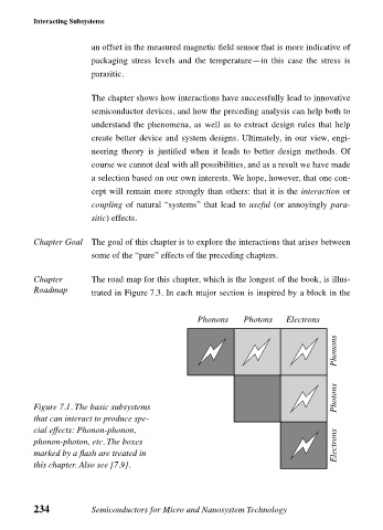
Chapter The road map for this chapter, which is the longest of the book, is illus-
Roadmap trated in Figure 7.3. In each major section is inspired by a block in the
Phonons Photons Electrons
Phonons
Photons
Figure 7.1. The basic subsystems
that can interact to produce spe-
cial effects: Phonon-phonon,
phonon-photon, etc. The boxes Electrons
marked by a flash are treated in
this chapter. Also see [7.9].
234 Semiconductors for Micro and Nanosystem Technology