
Page 326 - Semiconductor For Micro- and Nanotechnology An Introduction For Engineers
P. 326
Inhomogeneities
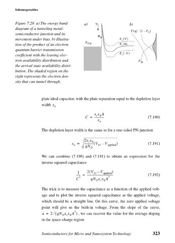
Figure 7.29. a) The energy band
diagram of a tunneling metal- a) η b)
T η() ( 1 F )
–
S
semiconductor junction and its
Φ
movement under bias. b) Illustra- B E V()
c
E
tion of the product of an electron FM E 0()
c
quantum barrier transmission
E –( V)
coefficient with the leaving elec- c
tron availability distribution and F M
the arrival state availability distri-
bution. The shaded region on the
right represents the electron den-
sity that can tunnel through.
plate ideal capacitor, with the plate separation equal to the depletion layer
width x
n
ε ε A
r 0
C = -------------- (7.190)
x
n
The depletion layer width is the same as for a one-sided PN-junction
2ε ε
r 0
x = ------------- V –( V ) (7.191)
n bi applied
qN D
We can combine (7.190) and (7.191) to obtain an expression for the
inverse squared capacitance
1 2 V –( bi V applied )
------ = -------------------------------------- (7.192)
2
2
C qN ε ε A
D r 0
The trick is to measure the capacitance as a function of the applied volt-
age and to plot the inverse squared capacitance as the applied voltage,
which should be a straight line. On this curve, the zero applied voltage
point will give us the built-in voltage. From the slope of the curve,
2
a = 2 (⁄ qN ε ε A ) , we can recover the value for the average doping
D r 0
in the space-charge region
Semiconductors for Micro and Nanosystem Technology 323