Page 321 - Semiconductor For Micro- and Nanotechnology An Introduction For Engineers
P. 321

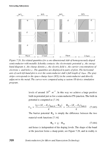
Interacting Subsystems
                       SCL
                              ψ          SCL ψ          SCL    E          SCL     E


                              E              E                  n                  n


                                                                p                  p
                              ρ              ρ


                             10µm         2.5µm              10µm            2.5µm
                Figure 7.26. Six related quantities for a one-dimensional slab of homogeneously-doped
                semiconductor with metallic Schottky contacts: the electrostatic potential  , the energy
                                                                           ψ
                band diagram  , the charge density  , the electric field  , the carrier concentrations of
                                             ρ
                            E
                                                             E
                electrons   and holes  . The quantities are displayed in pairs of plots. The horizontal
                                  p
                        n
                axis of each left-hand plot is over the semiconductor slab’s full length of 10µm  . The gray
                stripe corresponds to the space-charge layer (SCL) in the semiconductor and directly
                adjacent to the metal. The curves were computed using a custom 1D device simulation
                program.
                                                25  – 3
                               levels of around  10  m  . In this way we achieve a large positive
                               built-in potential just as for a semiconductor PN-junction. The built-in
                               potential is computed as [7.16]

                                     ( χ +  ( E –  E )  –  Φ )  Φ –  ( E –  E )
                                           c
                                                         M
                                                                     c
                                                               B
                                               F Bulk Si
                                                                         F Bulk Si
                               V   =  ----------------------------------------------------------------- =  --------------------------------------------------  (7.183)
                                 bi
                                               q                      q
                               The barrier potential  Φ   is simply the difference between the two
                                                   B
                               material work functions [7.16]
                                                 Φ B  =  χΦ M                    (7.184)
                                                        –
                               and hence is independent of the doping levels. The shape of the band
                               at the junction forms a sharp point, see Figure 7.28, and in reality is
                318          Semiconductors for Micro and Nanosystem Technology
   316   317   318   319   320   321   322   323   324   325   326