
Page 319 - Semiconductor For Micro- and Nanotechnology An Introduction For Engineers
P. 319
Interacting Subsystems
E E ∆E im
– qEx
E
E F x im x E F
x x
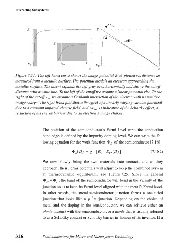
Figure 7.24. The left-hand curve shows the image potential Ex() plotted vs. distance as
measured from a metallic surface. The potential models an electron approaching the
metallic surface. The insert expands the left gray area horizontally and shows the cutoff
distance with a white line. To the left of the cutoff we assume a linear potential rise. To the
right of the cutoff x we assume a Coulomb interaction of the electron with its positive
im
image charge. The right-hand plot shows the effect of a linearly varying vacuum potential
due to a constant imposed electric field, and ∆E is indicative of the Schottky effect, a
im
reduction of an energy barrier due to an electron’s image charge.
The position of the semiconductor’s Fermi level w.r.t. the conduction
band edge is defined by the impurity doming level. We can write the fol-
lowing equation for the work function Φ of the semiconductor [7.16]
S
–
D
Φ D() = χ [ E – E ()] (7.182)
S c FS
We now slowly bring the two materials into contact, and as they
approach, their Fermi potentials will adjust to keep the combined system
at thermodynamic equilibrium, see Figure 7.25. Since in general
Φ ≠ Φ , the band of the semiconductor will bend in the vicinity of the
M S
junction so as to keep its Fermi level aligned with the metal’s Fermi level.
In other words, the metal-semiconductor junction forms a one-sided
++
junction that looks like a p n junction. Depending on the choice of
metal and the doping in the semiconductor, we can achieve either an
ohmic contact with the semiconductor, or a diode that is usually referred
to as a Schottky contact or Schottky barrier in honour of its inventor. If a
316 Semiconductors for Micro and Nanosystem Technology