Page 316 - Semiconductor For Micro- and Nanotechnology An Introduction For Engineers
P. 316

Inhomogeneities
                                                                           -
                                                                         +
                                                                   ε
                                                     1
                                                                           a
                                                                         d
                               C =  dQ   ----------------------------------------------------------------------    N N q  (7.179)
                                    ------- =
                                                                   --- -------------------------
                                    dV                      2k T   2   ( N +  N )
                                                                        -
                                                                             +
                                                              B
                                           ( V )   − V Applied  –  -------------  a  d
                                                   +
                                             bi Abrupt
                                                              q
                             for the abrupt junction.
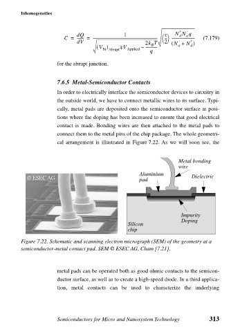
                             7.6.5 Metal-Semiconductor Contacts
                             In order to electrically interface the semiconductor devices to circuitry in
                             the outside world, we have to connect metallic wires to its surface. Typi-
                             cally, metal pads are deposited onto the semiconductor surface at posi-
                             tions where the doping has been increased to ensure that good electrical
                             contact is made. Bonding wires are then attached to the metal pads to
                             connect them to the metal pins of the chip package. The whole geometri-
                             cal arrangement is illustrated in Figure 7.22. As we will soon see, the
                                                                        Metal bonding
                                                                        wire
                                                          Aluminium
                  © ESEC AG                                                  Dielectric
                                                          pad


                                                                         Impurity
                                                                         Doping
                                                      Silicon
                                                      chip

                Figure 7.22. Schematic and scanning electron micrograph (SEM) of the geometry at a
                semiconductor-metal contact pad. SEM © ESEC AG, Cham [7.21].


                             metal pads can be operated both as good ohmic contacts to the semicon-
                             ductor surface, as well as to create a high-speed diode. In a third applica-
                             tion, metal contacts can be used to characterize the underlying


                             Semiconductors for Micro and Nanosystem Technology    313
   311   312   313   314   315   316   317   318   319   320   321