
Page 315 - Semiconductor For Micro- and Nanotechnology An Introduction For Engineers
P. 315
Interacting Subsystems
Adding these two expressions together yields the Shockley ideal diode
equation
J = J ( x ) + J ( – x )
P n N p
D D qV
Applied
P
N
= q ------- p n0 + -------n exp --------------------- – 1
p0
L P L N k T (7.177)
B
qV Applied
= J exp --------------------- – 1
0 k T
B
where the reverse saturation current density is
{
J = qp D ⁄ L + n D ⁄ L } . Equation (7.177) is plotted in
n0
p0
0
P
P
N
N
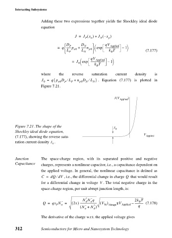
Figure 7.21.
(
JV )
Applied
Figure 7.21. The shape of the
J
0
Shockley ideal diode equation,
V
(7.177), showing the reverse satu- Applied
ration current density J .
0
Junction The space-charge region, with its separated positive and negative
Capacitance charges, represents a nonlinear capacitor, i.e., a capacitance dependent on
the applied voltage. In general, the nonlinear capacitance is defined as
⁄
C = dQ dV , i.e., the differential change in charge Q that would result
for a differential change in voltage V . The total negative charge in the
space-charge region, per unit abrupt junction length, is:
+ -
N N q 2k T
- d a − B
Q = qx N = ( 2ε) ------------------------- ( V ) + V Applied – ------------- (7.178)
P
a
bi Abrupt
+
-
( N + N ) q
a d
The derivative of the charge w.r.t. the applied voltage gives
312 Semiconductors for Micro and Nanosystem Technology