Page 310 - Semiconductor For Micro- and Nanotechnology An Introduction For Engineers
P. 310
Inhomogeneities
                                                   (
                                                     bi Abrupt
                                       x (  2  )  =  2ε V )     N a -           (7.164a)
                                                 ------------------------------ --------------------------------
                                        N abrupt
                                                                     -
                                                     q       + (  +  N )
                                                            N N +    a
                                                                d
                                                             d
                                                2ε V )          N +
                                                   (
                                                                 d
                                                     bi Abrupt
                                       x (  2  )  =  ------------------------------ --------------------------------  (7.164b)
                                        P abrupt             -  -    +
                                                     q     N N +   N )
                                                              (
                                                             a  a    d
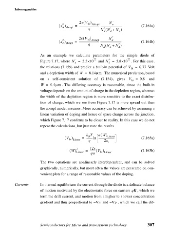
                             As an example we calculate parameters for the simple diode of
                                               -        22      +        22
                             Figure 7.17, where  N =  2.5×10   and  N =  5.8×10  . For this case,
                                              a                 d
                             the relations (7.159) and predict a built-in potential of  V  =  0.77  Volt
                                                                           bi
                             and a depletion width of W =  0.14µm  . The numerical prediction, based
                             on a self-consistent solution of (7.154), gives  V  =  0.8   and
                                                                           bi
                             W =  0.4µm  .  The differing accuracy is reasonable, since the built-in
                             voltage depends on the amount of charge in the depletion region, whereas
                             the width of the depletion region is more sensitive to the exact distribu-
                             tion of charge, which we see from Figure 7.17 is more spread out than
                             the abrupt model assumes. More accuracy can be achieved by assuming a
                             linear variation of doping and hence of space charge across the junction,
                             which Figure 7.17 confirms to be closer to reality. In this case we do not
                             repeat the calculations, but just state the results
                                                           (
                                                    k T   aW)
                                                     B
                                                               Linear
                                         ( V )    =  ---------ln  ------------------------  (7.165a)
                                           bi Linear
                                                     q       2n i
                                            ( W) 3 Linear  =  12ε (             (7.165b)
                                                      --------- V )
                                                      qa   bi Linear
                             The two equations are nonlinearly interdependent, and can be solved
                             graphically, numerically, but most often the values are presented on con-
                             venient plots for a range of reasonable values of the doping.
                Currents     In thermal equilibrium the current through the diode is a delicate balance
                             of motion motivated by the electrostatic force on carriers qE  , which we
                             term the drift current, and motion from a higher to a lower concentration
                             gradient and thus proportional to  ∇–  n   and  ∇–  p  , which we call the dif-


                             Semiconductors for Micro and Nanosystem Technology    307

