Page 309 - Semiconductor For Micro- and Nanotechnology An Introduction For Engineers
P. 309
Interacting Subsystems
Abrupt
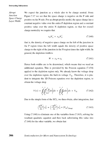
Junction We expect the junction as a whole also to be charge neutral. From
Figure 7.17 we see that the space charge is negative on the P side and
Space Charge
positive on the N side. For an abrupt profile model, the space charge has a
Layer Width
constant negative value over the entire P depletion region and a constant
positive value over the entire N depletion region, so that for overall
charge neutrality we require that
- +
x N = x N (7.160)
P a N d
that is, the density of negative space charge on the left of the junction in
the P region times the left width equals the density of positive space
charge to the right of the junction in the N region times the right width. In
general, the depletion width is
W = x + x (7.161)
N P
Hence both widths are to be determined, which means that we need an
additional equation. This is provided by the Poisson equation (7.154)
applied to the depletion region only. We already know the voltage drop
over the depletion region, the built-in voltage V . Therefore, it is pru-
bi
dent to integrate the 1D Poisson equation over the depletion region, to
obtain the voltage drop
x x x x
2
∂ ψ
Vx() = ∫ ∫ --------- xd xd = ∫ ∫ ρ x xd = V bi (7.162)
d
∂x 2
0 0 0 0
Due to the simple form of the SCL, we then obtain, after integration, that
- -
qN a 2 – qN a 2 ( V )
------------- x +
---------- x =
2ε P 2ε N bi Abrupt (7.163)
Using (7.160) to eliminate one of the variables from (7.163), solving the
resultant quadratic equation and then back substituting this value into
(7.160) for the other variable, we obtain that
306 Semiconductors for Micro and Nanosystem Technology

