Page 305 - Semiconductor For Micro- and Nanotechnology An Introduction For Engineers
P. 305

Interacting Subsystems
                Unbiased
                                                                                2
                Junction     For an unbiased junction, we expect charge neutrality at distances far . 0
                             from the junction where the potential is constant, i.e., where ∇ ψ =
                             This can be expressed as
                                                     +       -
                                                p +  N =  n +  N                 (7.151)
                                                     d       a
                             i.e., the sum of the number of holes and ionized donors (the positive
                             charges in the crystal) must equal the sum of the number of electrons and
                             ionized acceptors. The ionization is governed by fermion statistics, which
                             leads us to write (7.151) as

                                               – E F       N d
                                         N Exp ---------(  ) +  ----------------------------------------------
                                          c
                                               k T           E –  E
                                                B              d   F
                                                     1 +  Exp -------------------–(  )
                                                               k T
                                                                B
                                                                              (7.152a)
                                              E –  E g       N a     
                                                F
                                      =   N Exp ------------------(  ) +  ------------------------------------------
                                          v
                                               k T            E –  E F 
                                                 B
                                                                 a
                                                       1 +  Exp ------------------(  k T  ) 
                                                                  B
                                                      3                     3
                                                      ---                   ---
                                                                       h B 
                                                 e B 
                                             2πm k T 2            2πm k T 2
                                where N =  2 -----------------------   and N =  2 -----------------------   (7.153a)
                                            
                                                                  
                                       c
                                                             v
                                                                       2
                                                 2
                                                h                     h
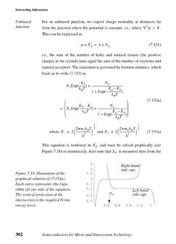
                             This equation is nonlinear in  E F   and must be solved graphically (see
                             Figure 7.18) or numerically. Also note that E F   is measured here from the
                                                    3
                                                                   Right-hand
                                                    2              side eqn.
                Figure 7.18. Illustration of the   1.5
                graphical solution of (7.152a).     1
                Each curve represents (the loga-   0.7
                rithm of) one side of the equation.   0.5                Left-hand
                                                              E
                The vertical projection of the     0.3         F         side eqn.
                intersection is the required Fermi   0.2
                energy level.                         0    0.2  0.4   0.6  0.8    1

                302          Semiconductors for Micro and Nanosystem Technology
   300   301   302   303   304   305   306   307   308   309   310