Page 303 - Semiconductor For Micro- and Nanotechnology An Introduction For Engineers
P. 303
Interacting Subsystems
2
∂ f z()
c
l
2
2
------------------ – ( k α) f z() = 0 α = 1 – ------- 2 (7.145b)
c
l
2
2
∂z β1
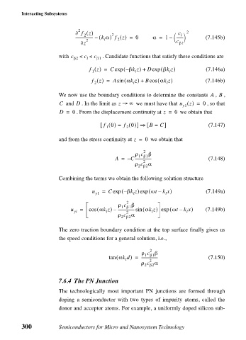
with c β2 < c < c β1 . Candidate functions that satisfy these conditions are
l
f z() = Cexp – ( βk z) + Dexp ( βk z) (7.146a)
1
l
l
f z() = Asin ( αk z) + Bcos ( αk z) (7.146b)
2 l l
We now use the boundary conditions to determine the constants , ,
AB
z
C and D . In the limit as z → ∞ we must have that u () = 0 , so that
y1
D = 0 . From the displacement continuity at z = 0 we obtain that
[ f 0() = f 0()] ⇒ [ B = C] (7.147)
1 2
and from the stress continuity at z = 0 we obtain that
2
ρ c β
1 β1
A = – C----------------- (7.148)
2
ρ c α
2 β2
Combining the terms we obtain the following solution structure
u = Cexp – ( βk z)exp ( ωt – k x) (7.149a)
y1 l l
2
ρ c β
1 β1
u = cos ( αk z) – -----------------sin ( αk z) exp ( ωt – k x) (7.149b)
yi l 2 l l
ρ c α
2 β2
The zero traction boundary condition at the top surface finally gives us
the speed conditions for a general solution, i.e.,
2
ρ c β
1 β1
tan ( αk d) = ----------------- (7.150)
l 2
ρ c α
2 β2
7.6.4 The PN Junction
The technologically most important PN junctions are formed through
doping a semiconductor with two types of impurity atoms, called the
donor and acceptor atoms. For example, a uniformly doped silicon sub-
300 Semiconductors for Micro and Nanosystem Technology

