Page 308 - Semiconductor For Micro- and Nanotechnology An Introduction For Engineers
P. 308
Inhomogeneities
• If we assume that the doping profile at the junction within the SCL is
linear, which is in fact quite reasonable, then the space-charge is also
linear, making the electric field quadratic and the electric potential a
piece-wise cubic function within the profile.
Abrupt From the abrupt junction model we can quickly estimate the width of the
Junction SCL and the value of the built-in potential. From the relation for the
Built-in
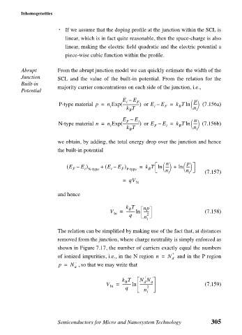
majority carrier concentrations on each side of the junction, i.e.,
Potential
E – E F
p
i
P-type material p = n Exp -----------------( ) or E – E = k T ln ---- (7.156a)
i i F B n
k T
B i
E – E i
n
F
N-type material n = n Exp -----------------( ) or E – E = k T ln ---- (7.156b)
i F i B n
k T i
B
we obtain, by adding, the total energy drop over the junction and hence
the built-in potential
p
n
( E – E ) + ( E – E ) = k T ln ln
----
---- +
n
F
B
i
i N-type
F P-type
i n (7.157)
i
= qV bi
and hence
k T np
B
V = ---------ln ------ (7.158)
bi 2
q n
i
The relation can be simplified by making use of the fact that, at distances
removed from the junction, where charge neutrality is simply enforced as
shown in Figure 7.17, the number of carriers exactly equal the numbers
+
of ionized impurities, i.e., in the N region n = N and in the P region
d
-
p = N , so that we may write that
a
+ -
k T N N a
d
B
V bi = ---------ln -------------- (7.159)
q n 2
i
Semiconductors for Micro and Nanosystem Technology 305

