
Page 312 - Semiconductor For Micro- and Nanotechnology An Introduction For Engineers
P. 312
Inhomogeneities
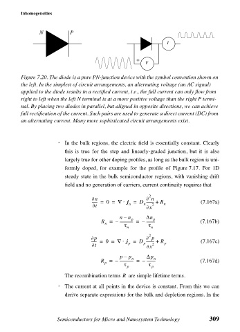
N
P
I
+
V
Figure 7.20. The diode is a pure PN-junction device with the symbol convention shown on
the left. In the simplest of circuit arrangements, an alternating voltage (an AC signal)
applied to the diode results in a rectified current, i.e., the full current can only flow from
right to left when the left N terminal is at a more positive voltage than the right P termi-
nal. By placing two diodes in parallel, but aligned in opposite directions, we can achieve
full rectification of the current. Such pairs are used to generate a direct current (DC) from
an alternating current. Many more sophisticated circuit arrangements exist.
• In the bulk regions, the electric field is essentially constant. Clearly
this is true for the step and linearly-graded junction, but it is also
largely true for other doping profiles, as long as the bulk region is uni-
formly doped, for example for the profile of Figure 7.17. For 1D
steady state in the bulk semiconductor regions, with vanishing drift
field and no generation of carriers, current continuity requires that
2
∂n ∂ n
------ = 0 = ∇ j ⋅ n = D -------- + R n (7.167a)
n
∂t ∂x 2
–
nn p ∆n p
R = – -------------- = – --------- (7.167b)
n
τ
n τ n
2
∂p ∂ p
------ = 0 = ∇ j ⋅ p = D --------- + R p (7.167c)
p
∂t ∂x 2
p – p n ∆p n
R = – --------------- = – --------- (7.167d)
p τ τ
p p
The recombination terms are simple lifetime terms.
R
• The current at all points in the device is constant. From this we can
derive separate expressions for the bulk and depletion regions. In the
Semiconductors for Micro and Nanosystem Technology 309