Page 314 - Semiconductor For Micro- and Nanotechnology An Introduction For Engineers
P. 314
Inhomogeneities
2
n
i
(
(
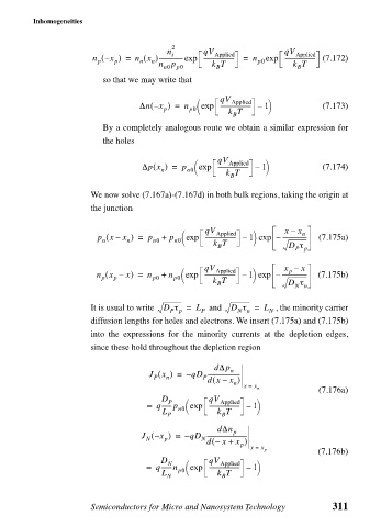
n – x ) = n x )----------------exp qV Applied n exp qV Applied (7.172)
--------------------- =
---------------------
p
n
n
p0
p
n p k T k T
n0 p0 B B
so that we may write that
(
∆n – x ) = n p0 exp qV Applied 1 (7.173)
--------------------- –
p
k T
B
By a completely analogous route we obtain a similar expression for
the holes
(
--------------------- –
∆px ) = p n0 exp qV Applied 1 (7.174)
n
k T
B
We now solve (7.167a)-(7.167d) in both bulk regions, taking the origin at
the junction
x
x –
n
(
--------------------- –
p x – x ) = p + p exp qV Applied 1 exp – ----------------- (7.175a)
n n n0 n0 k T D τ
B
P p
x –
x
p
(
--------------------- –
n x – x) = n p0 + n p0 exp qV Applied 1 exp – ----------------- (7.175b)
p
p
k T
B D τ
N n
It is usual to write D τ = L P and D τ = L N , the minority carrier
P p
N n
diffusion lengths for holes and electrons. We insert (7.175a) and (7.175b)
into the expressions for the minority currents at the depletion edges,
since these hold throughout the depletion region
d∆p n
J ( x ) = – qD ----------------------
P n P ( x )
dx – n
x = x n
(7.176a)
D P qV Applied
= q------- p n0 exp --------------------- – 1
L k T
P B
d∆n p
J ( – x ) = – qD ---------------------------
N
(
N
p
d – + x )
x
p
x = x p
(7.176b)
D N qV Applied
= q-------n p0 exp --------------------- – 1
L N k T
B
Semiconductors for Micro and Nanosystem Technology 311

