
Page 317 - Semiconductor For Micro- and Nanotechnology An Introduction For Engineers
P. 317
Interacting Subsystems
semiconductor surface and extract parameters such as the doping concen-
tration.
Work An electron taken from an infinitely removed position in vacuum towards
Function a clean metallic surface that is at the Fermi potential of the ensemble of
metallic valence electrons, needs to pass through a potential, called the
work function Φ , that is a fundamental property of the metal. It is sim-
M
ply equal to the work required to move an electron from the Fermi level
to an energy level where it is free from the crystal. The Fermi surface of
the metal represents a “sea” of non-localized valence electrons that are
available for conduction, unhampered by a forbidden bandgap. Typical
values of metallic work functions are Φ = 4.25eV , Φ = 4.5eV
Al W
and Φ = 5.3eV .
Pt
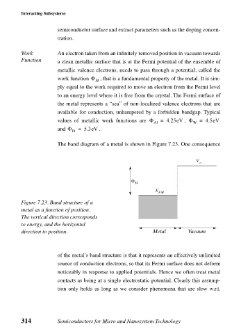
The band diagram of a metal is shown in Figure 7.23. One consequence
V o
Φ M
E FM
Figure 7.23. Band structure of a
metal as a function of position.
The vertical direction corresponds
to energy, and the horizontal
direction to position. Metal Vacuum
of the metal’s band structure is that it represents an effectively unlimited
source of conduction electrons, so that its Fermi surface does not deform
noticeably in response to applied potentials. Hence we often treat metal
contacts as being at a single electrostatic potential. Clearly this assump-
tion only holds as long as we consider phenomena that are slow w.r.t.
314 Semiconductors for Micro and Nanosystem Technology