
Page 318 - Semiconductor For Micro- and Nanotechnology An Introduction For Engineers
P. 318
Inhomogeneities
metallic relaxation times. If we bring the electron close to the metallic
surface, we notice an interesting effect.
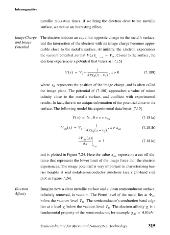
Image Charge The electron induces an equal but opposite charge on the metal’s surface,
and Image and the interaction of the electron with its image charge becomes appre-
Potential
ciable close to the metal’s surface. At infinity, the electron experiences
the vacuum potential, so that Vx() = V . Closer to the surface, the
x → ∞ 0
electron experiences a potential that varies as [7.15]
1
Vx() = V – ------------------------------- , x > 0 (7.180)
0
4πε x –(
0
0 x )
where x represents the position of the image charge, and is often called
0
the image plane. The potential of (7.180) approaches a value of minus
infinity close to the metal’s surface, and conflicts with experimental
results. In fact, there is no unique information of the potential close to the
surface. The following model fits experimental data better [7.15]
Vx() = lx , 0 >> x (7.181a)
x
im
1
x
V () = V – ------------------------------- , x > x im (7.181b)
0
im
4πε x –(
0 x )
0
∂V ()
x
im
-------------------- = l (7.181c)
∂x
x im
and is plotted in Figure 7.24. Here the value x represents a cut-off dis-
im
tance that represents the lower limit of the image force that the electron
experiences. The image potential is very important in characterizing bar-
rier heights at real metal-semiconductor junctions (see right-hand side
plot in Figure 7.24).
Electron Imagine now a clean metallic surface and a clean semiconductor surface,
Affinity infinitely removed, in vacuum. The Fermi level of the metal lies at Φ
M
below the vacuum level V . The semiconductor’s conduction band edge
0
χ
χ
lies at a level below the vacuum level V . The electron affinity is a
0
fundamental property of the semiconductor, for example χ = 4.05eV .
Si
Semiconductors for Micro and Nanosystem Technology 315