
Page 322 - Semiconductor For Micro- and Nanotechnology An Introduction For Engineers
P. 322
Inhomogeneities
a)
V 0 V 0 b) V 0
V 0
Φ Φ χ S Φ S χ S
Φ M B S Φ M
E c
E E c E
FM FM
E FS E FS
E – E FS E v E – E FS
c
c
E v
Metal Si Metal Si
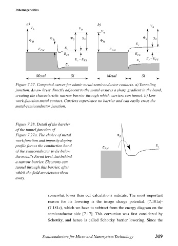
Figure 7.27. Computed curves for ohmic metal-semiconductor contacts. a) Tunneling
junction. An n+ layer directly adjacent to the metal ensures a sharp gradient in the band,
creating the characteristic narrow barrier through which carriers can tunnel. b) Low
work-function metal contact. Carriers experience no barrier and can easily cross the
metal-semiconductor junction.
Figure 7.28. Detail of the barrier
of the tunnel junction of
Figure 7.27a. The choice of metal Φ B
work function and impurity doping
profile forces the conduction band E
E FM c
of the semiconductor to lie below
the metal’s Fermi level, but behind
a narrow barrier. Electrons can
tunnel through this barrier, after
which the field accelerates them
away.
somewhat lower than our calculations indicate. The most important
reason for its lowering is the image charge potential, (7.181a)-
(7.181c), which we have to subtract from the energy diagram on the
semiconductor side [7.17]. This correction was first considered by
Schottky, and hence is called Schottky barrier lowering. Since the
Semiconductors for Micro and Nanosystem Technology 319