
Page 320 - Semiconductor For Micro- and Nanotechnology An Introduction For Engineers
P. 320
Inhomogeneities
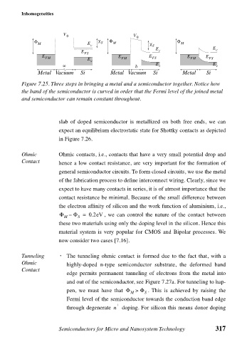
Φ M V 0 E χ S Φ M V 0 χ Φ M
c S
E E
E c c
E FS E E E E
FM E v FM FS FM FS
∞ δ E v E v
Metal Vacuum Si Metal Vacuum Si Metal Si
Figure 7.25. Three steps in bringing a metal and a semiconductor together. Notice how
the band of the semiconductor is curved in order that the Fermi level of the joined metal
and semiconductor can remain constant throughout.
slab of doped semiconductor is metallized on both free ends, we can
expect an equilibrium electrostatic state for Shottky contacts as depicted
in Figure 7.26.
Ohmic Ohmic contacts, i.e., contacts that have a very small potential drop and
Contact hence a low contact resistance, are very important for the formation of
general semiconductor circuits. To form closed circuits, we use the metal
of the fabrication process to define interconnect wiring. Clearly, since we
expect to have many contacts in series, it is of utmost importance that the
contact resistance be minimal. Because of the small difference between
the electron affinity of silicon and the work function of aluminium, i.e.,
Φ – Φ = 0.2eV , we can control the nature of the contact between
M S
these two materials using only the doping level in the silicon. Hence this
material system is very popular for CMOS and Bipolar processes. We
now consider two cases [7.16].
Tunneling • The tunneling ohmic contact is formed due to the fact that, with a
Ohmic highly-doped n-type semiconductor substrate, the deformed band
Contact
edge permits permanent tunneling of electrons from the metal into
and out of the semiconductor, see Figure 7.27a. For tunneling to hap-
pen, we must have that Φ > Φ . This is achieved by raising the
M S
Fermi level of the semiconductor towards the conduction band edge
+
through degenerate n doping. For silicon this means donor doping
Semiconductors for Micro and Nanosystem Technology 317