
Page 306 - Semiconductor For Micro- and Nanotechnology An Introduction For Engineers
P. 306
Inhomogeneities
edge of the valence band. Once we have obtained either the Fermi level
or the potential in the device, we can easily compute the other quantities
required for the band diagram, as was done for Figure 7.17.
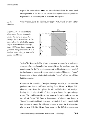
At the We now zoom in on the junction, see Figure 7.19, which is where all the
Junction
SCL
Figure 7.19. The labeled band
diagram at the junction of the
E d
diode. The vertical axis is the
energy, the horizontal axis is dis-
E
tance along the diode. The shaded E g c
region marks the space-charge
E F
layer (SCL) that forms around the E
v
junction. The junction results in a E i
qV bi
built-in potential V at thermody-
bi E a
namic equilibrium.
“action” is. Because the Fermi level is constant in a material, a basic con-
sequence of thermodynamics, but removed from the band-gap center in
doped materials, the PN junction causes a transition in the energy level of
the band edge as we move from one side to the other. This energy “jump”
is associated with an electrostatic potential “jump”, which we call the
built-in potential.
Carriers on the two sides of the junction experience large concentration
gradients and hence a diffusion driving force. Hence, in Figure 7.19,
electrons move from the right to the left, and holes from left to right,
leaving the vicinity devoid of free charges, hence the space-charge
region. The resulting positive region on the right and negative region on
the left of Figure 7.19 form a double-layer of charges and hence a
“hump” in electric field pointing from right to left. It is this electric field
that eventually causes the diffusion process to stop, for it acts on the
charges as a drift-like driving force opposing the diffusion current. An
Semiconductors for Micro and Nanosystem Technology 303