
Page 304 - Semiconductor For Micro- and Nanotechnology An Introduction For Engineers
P. 304
Inhomogeneities
strate, e.g., with the donor arsenic (As), is subsequently doped with the
acceptor boron (B), in select regions, to form PN junctions. We will not
concern ourselves with the fabrication methods of PN junctions, but it is
important to note that they have a strong influence on the spatial distribu-
tion of foreign ions in the silicon lattice. More important for the analysis
here is the level of doping. It is technologically possible to vary the con-
20 26
centration level of foreign dopants in the range 10 – 10 atoms per
21 24
cubic meter; typical values, however, are 10 – 10 dopant atoms per
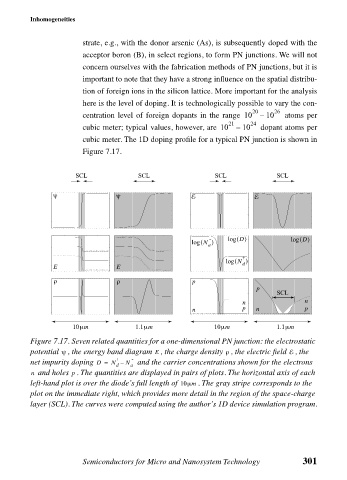
cubic meter. The 1D doping profile for a typical PN junction is shown in
Figure 7.17.
SCL SCL SCL SCL
ψ ψ E E
D
D
- log () log ()
log ( N )
a
+
log ( N )
d
E E
ρ ρ p
p
SCL
n n
n p n p
10µm 1.1µm 10µm 1.1µm
Figure 7.17. Seven related quantities for a one-dimensional PN junction: the electrostatic
potential , the energy band diagram , the charge density , the electric field , the
ρ
ψ
E
E
+ -
net impurity doping D = N – N a and the carrier concentrations shown for the electrons
d
n and holes . The quantities are displayed in pairs of plots. The horizontal axis of each
p
left-hand plot is over the diode’s full length of 10µm . The gray stripe corresponds to the
plot on the immediate right, which provides more detail in the region of the space-charge
layer (SCL). The curves were computed using the author’s 1D device simulation program.
Semiconductors for Micro and Nanosystem Technology 301