Page 299 - Semiconductor For Micro- and Nanotechnology An Introduction For Engineers
P. 299
Interacting Subsystems
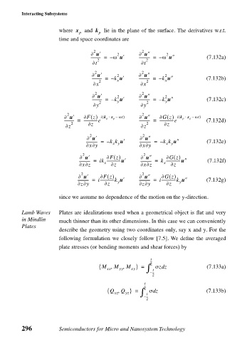
                                             lie in the plane of the surface. The derivatives w.r.t.
                             where  x
                                      and  k
                                    p
                                           p
                             time and space coordinates are
                                         2
                                                          2
                                        ∂ u′     2       ∂ u″     2
                                        ---------- =  – ω u′  ----------- =  – ω u″  (7.132a)
                                                           2
                                          2
                                        ∂t               ∂t
                                         2
                                                          2
                                        ∂ u′     2       ∂ u″     2
                                        ---------- =  k – u′  ----------- =  k – u″  (7.132b)
                                           2     x         2      x
                                         ∂x              ∂x
                                         2
                                                          2
                                        ∂ u′     2       ∂ u″     2
                                        ---------- =  k – u′  ----------- =  k – u″  (7.132c)
                                                                  y
                                                 y
                                                           2
                                           2
                                         ∂y              ∂y
                                                          2
                               2
                              ∂ u′   ∂Fz() i k p x p –(  ⋅  ωt)  ∂ u″  ∂Gz() i k p x p –(  ⋅  ωt)
                              ---------- =  --------------e  ----------- =  ---------------e  (7.132d)
                                                           2
                                 2
                               ∂z      ∂z                ∂z      ∂z
                                       2
                                                          2
                                      ∂ u′               ∂ u″
                                      ------------ =  – k k u′  ------------ =  – k k u″  (7.132e)
                                               x y
                                                                  x y
                                      ∂x∂y               ∂x∂y
                                     2
                                                          2
                                    ∂ u′     ∂Fz()       ∂ u″     ∂Gz()
                                    ------------ =  ik --------------u′  ------------ =  k ---------------u″  (7.132f)
                                                                 x
                                             x
                                    ∂x∂z       ∂z        ∂x∂z       ∂z
                                    2
                                                          2
                                   ∂ u′    ∂Fz()         ∂ u″    ∂Gz()
                                   ------------ =  i--------------k u′  ------------ =  i---------------k u″  (7.132g)
                                                 y
                                                                       y
                                   ∂z∂y      ∂z          ∂z∂y     ∂z
                             since we assume no dependence of the motion on the y-direction.
                Lamb Waves   Plates are idealizations used when a geometrical object is flat and very
                in Mindlin   much thinner than its other dimensions. In this case we can conveniently
                Plates
                             describe the geometry using two coordinates only, say x and y. For the
                             following formulation we closely follow [7.5]. We define the averaged
                             plate stresses (or bending moments and shear forces) by
                                                             t
                                                             ---
                                          { M ,  M ,  M } =  2 t ∫  σzz         (7.133a)
                                                                 d
                                             xx
                                                  yy
                                                      xy
                                                             – ---
                                                             2
                                                           t
                                                          ---
                                             { Q ,  Q } =  2 t ∫  σ z           (7.133b)
                                                             d
                                                xz
                                                    yz
                                                          – ---
                                                           2
                296          Semiconductors for Micro and Nanosystem Technology

