Page 301 - Semiconductor For Micro- and Nanotechnology An Introduction For Engineers
P. 301
Interacting Subsystems
∂Q
xz
∂y ∫
----------- +
d
---------- zd =
----------- + ∂Q yz --- 2 t ∂σ zz ρ t --- 2 t ∫ u˙˙ z (7.137c)
z
∂x – --- t ∂z – ---
2 2
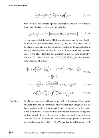
Next we make the Mindlin-specific assumption about the deformation
through the thickness of the plate, namely that
,,
u u u ( xy z) = zU xy,( ) zU xy) Wx y) , (7.138)
(
,
,
(
x y z x y
i.e., we assume that the entire 3D deformation field can be described by
the three averaged deformation values U , U and W defined only in
x y
the plane of the plate, and that variation of the lateral deflection (in the x-
and y-directions) depends linearly on the distance from this “neutral”
plane of the plate. Inserting this assumption and the plate constitutive
relations (7.135a)–(7.136b) into (7.137a)–(7.137b) give the isotropic
plate equations of motion
2
∂ U 2 ∂W
x
(
------------ +
D 1 + ν) ------------ + ∂ U y ( 1 – ν)∇ 2 U – µ′hU + --------
x
x
∂x 2 ∂x∂y ∂x (7.139a)
ρ 3
˙˙
= ------h U x
12
∂ε ∂ε +( νε ) ρ 3
xx
xy
yy
˙˙
(
D 1 – ν)---------- + D-------------------------------- – µ′hR yz = ------h U y (7.139b)
∂x ∂y 12
t --- t ---
∂R xz ∂R yz 2 ∂σ zz 2
∂y ∫
d
µ′h ----------- + ----------- + ---------- zd = ρ t ∫ u˙˙ z (7.139c)
∂x – --- t ∂z – --- z
2 2
Love Waves By placing a thin material layer such as silicon dioxide or silicon nitride
on a semi-infinite half-space made of silicon (or thick enough so that the
theory applies) we form a waveguide for the surface waves. In fact, many
of the mathematical techniques used for optical waveguides are applica-
ble here as well. To keep this section as short as possible, we only con-
sider one layer on top of the half space, even though practical situations
may involve more layers [7.5], [7.6]. We number the substrate as i = 1
298 Semiconductors for Micro and Nanosystem Technology

