
Page 48 - Semiconductor For Micro- and Nanotechnology An Introduction For Engineers
P. 48
Crystal Structure
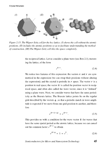
(II)
(I)
(III)
Figure 2.15. The Wigner-Seitz cell for the bcc lattice. (I) shows the cell without the atomic
positions. (II) includes the atomic positions so as to facilitate understanding the method
of construction. (III) The Wigner-Seitz cell tiles the space completely.
the reciprocal lattice. Let us consider a plane wave (see Box 2.1), travers-
ing the lattice, of the form
•
ikr
e . (2.4)
We notice two features of this expression: the vectors and are sym-
r
k
metrical in the expression (we can swap their positions without altering
r
r
the expression); and the crystal is periodic in space. The vector is a
position in real space; the vector is called the position vector in recip-
k
rocal space, and often also called the wave vector, since it is “defined”
using a plane wave. Next, we consider waves that have the same period-
icity as the Bravais lattice. The Bravais lattice points lie on the regular
grid described by the vectors , so that a periodic match in wave ampli-
q
tude is expected if we move from one grid position to another, and there-
fore
•
•
ik ( r + q) ikr
e = e . (2.5)
This provides us with a condition for the wave vector for waves that
k
have the same spatial period as the atomic lattice, because we can cancel
•
ikr
out the common factor e to obtain
•
ikq 0
e = 1 = e . (2.6)
Semiconductors for Micro and Nanosystem Technology 45