Page 91 - Semiconductor For Micro- and Nanotechnology An Introduction For Engineers
P. 91
The Crystal Lattice System
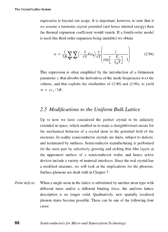
expression is beyond our scope. It is important, however, to note that it
we assume a harmonic crystal potential (and hence internal energy) then
the thermal expansion coefficient would vanish. If a fourth-order model
is used (the third order expansion being unstable) we obtain
1 ∂ ∂ 1
α = ------- ∑ ∑ – -------—ω ------- --------------------------------------- (2.96)
k
3B ∂V ∂T E i
k i exp – --------- – 1
k T
B
This expression is often simplified by the introduction of a Grüneisen
γ
parameter that absorbs the derivatives of the mode frequencies w.r.t the
volume, and that exploits the similarities of (2.90) and (2.96), to yield
α = γc ⁄ 3B .
v
2.5 Modifications to the Uniform Bulk Lattice
Up to now we have considered the perfect crystal to be infinitely
extended in space, which enabled us to make a straightforward ansatz for
the mechanical behavior of a crystal atom in the potential field of the
electrons. In reality semiconductor crystals are finite, subject to defects,
and terminated by surfaces. Semiconductor manufacturing is performed
for the most part by selectively growing and etching thin film layers at
the uppermost surface of a semiconductor wafer, and hence active
devices include a variety of material interfaces. Since the real crystal has
a modified structure, we will look at the implications for the phonons.
Surface phonons are dealt with in Chapter 7.
Point defects When a single atom in the lattice is substituted by another atom type with
different mass and/or a different binding force, the uniform lattice
description is no longer valid. Qualitatively, new spatially localized
phonon states become possible. These can be one of the following four
cases:
88 Semiconductors for Micro and Nanosystem Technology

