
Page 92 - Semiconductor For Micro- and Nanotechnology An Introduction For Engineers
P. 92
Modifications to the Uniform Bulk Lattice
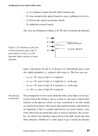
• A: at a frequency higher than the optical branch, and,
• B: close enough to the optical branch to cause a splitting of its levels;
• C: between the optical an acoustic branch;
• D: within the acoustic branch.
The cases are illustrated in Figure 2.29. We now reconsider the diatomic
A
B
Optical Branch
C
Figure 2.29. Positions of the four
Acoustic Branch
localized phonon states, due to D
point defects [2.12], on a 1D
diatomic lattice density-of-states
diagram.
lattice, with masses M and m , of Section 2.4.1 but with the mass of one
µ
site slightly perturbed, i.e., replaced with a mass . The four cases are:
• µ < m < M , mass of type m is replaced;
• m < µ < M , mass of type m is replaced, i.e., in the gap;
• m < µ < M , mass of type M is replaced, i.e., in the gap;
• m < M < µ , mass of type M is replaced.
Introducing The assumptions we have made about the bulk crystal lattice do not nec-
an Interface essarily hold at the interface, and as a result we can expect certain modi-
fications to the physical effects we have considered so far that should
account for its presence. One reason why material surfaces and interfaces
are important, is that we usually build devices on crystal surfaces; also,
many effects that are useful take place at material interfaces. By an inter-
face we denote that transition region between the bulk crystal and some
other substance, whether it is a solid, liquid or gas. Usually the interface
Semiconductors for Micro and Nanosystem Technology 89