
Page 94 - Semiconductor For Micro- and Nanotechnology An Introduction For Engineers
P. 94
Summary for Chapter 2
3 Dimer Atom
1 Intermediate layer atom
4 Rest Atom 2 1 3
2 Adatom 4
(b)
3
1
4
2
(a)
(c)
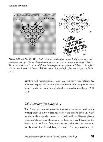
Figure 2.30. (a) The Si 111〈 〉 7 × 7 -reconstructed surface imaged with a scanning tun-
neling microscope. The overlay indicates the various atomic positions in the DAS layer.
The pictures (b) and (c) to the right are for comparison purposes, and show the first four
silicon atom layers. (c) Shows a 3-dimensional view of the first four atom layers of the lat-
tice.
quantum-well semiconductor lasers also represent superlattices. We
expect the superlattice to have a local influence on the dispersion curve
because additional waves are admitted with another wavelength [2.2],
[2.16].
2.6 Summary for Chapter 2
The forces between the constituent atoms of a crystal lead to the
pseudoparticle of lattice vibrational energy: the phonon. From this view,
we obtain the dispersion curves for a solid with its different phonon
branches. The acoustic phonons, in the long wavelength limit, are the
elastic waves we know from a macroscopic viewpoint, and we com-
pletely recover the classical theory of elasticity. The high frequency opti-
Semiconductors for Micro and Nanosystem Technology 91