
Page 272 - Semiconductor Manufacturing Handbook
P. 272
Geng(SMH)_CH18.qxd 04/04/2005 19:58 Page 18.13
WET CLEANING
WET CLEANING 18.13
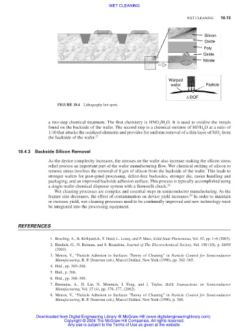
Silicon
Oxide
Poly
Oxide
Nitride
Warped
wafer Particle
∆ DOF
FIGURE 18.4 Lithography hot spots.
a two-step chemical treatment. The first chemistry is HNO /H O. It is used to oxidize the metals
3 2
found on the backside of the wafer. The second step is a chemical mixture of HF/H O at a ratio of
2
1:10 that attacks the oxidized elements and provides for uniform removal of a thin layer of SiO from
2
the backside of the wafer. 27
18.4.3 Backside Silicon Removal
As the device complexity increases, the stresses on the wafer also increase making the silicon stress
relief process an important part of the wafer manufacturing flow. Wet chemical etching of silicon to
remove stress involves the removal of 8 µm of silicon from the backside of the wafer. This leads to
stronger wafers for post-grind processing, defect-free backsides, stronger die, easier handling and
packaging, and an improved backside adhesion surface. This process is typically accomplished using
a single-wafer chemical dispense system with a Bernoulli chuck. 28
Wet cleaning processes are complex and essential steps in semiconductor manufacturing. As the
29
feature size decreases, the effect of contamination on device yield increases. In order to maintain
or increase yield, wet cleaning processes need to be continually improved and new technology must
be integrated into the processing equipment.
REFERENCES
1. Bowling, A., B. Kirkpatrick, T. Hurd, L. Losey, and P. Matz, Solid State Phenomena, Vol. 92, pp. 1–6 (2003).
2. Burdick, G., N. Berman, and S. Beaudoin, Journal of The Electrochemical Society, Vol. 150 (10), p. G659
(2003).
3. Menon, V., “Particle Adhesion to Surfaces: Theory of Cleaning” in Particle Control for Semiconductor
Manufacturing, R. P. Donovan (ed.), Marcel Dekker, New York (1990), pp. 362–365.
4. Ibid., pp. 365–366.
5. Ibid., p. 366.
6. Ibid., pp. 368–369.
7. Busnaina, A., H. Lin, N. Moumen, J. Feng, and J. Taylor, IEEE Transactions on Semiconductor
Manufacturing, Vol. 15 (4), pp. 376–377, (2002).
8. Menon, V., “Particle Adhesion to Surfaces: Theory of Cleaning” in Particle Control for Semiconductor
Manufacturing, R. P. Donovan (ed.), Marcel Dekker, New York (1990), p. 360.
Downloaded from Digital Engineering Library @ McGraw-Hill (www.digitalengineeringlibrary.com)
Copyright © 2004 The McGraw-Hill Companies. All rights reserved.
Any use is subject to the Terms of Use as given at the website.