
Page 277 - Semiconductor Manufacturing Handbook
P. 277
Geng(SMH)_CH19.qxd 04/04/2005 20:00 Page 19.4
INSPECTION, MEASUREMENT, AND TEST
19.4 FINAL MANUFACTURING
process enables a smaller chip to perform the same function thus enabling more chips to be built on
a wafer and partially offsetting the effect of the higher defect density on yield. The economics usually
work out such that the difference between the higher price commanded by the higher performance
chip and the lower wafer cost per chip more than makes up for the cost of the test and reduction in
yield. Therefore, manufacturing tests decrease product cost again by allowing the product to use a
higher density and lower quality process while maintaining acceptable customer quality.
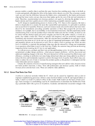
An IC design-to-manufacturing process is shown in Fig. 19.1. Since in this sequence, the later a
defect is found after it is created, the more the wasted effort and material, it is advisable to perform
tests at each level of assembly. However, each test instance needs only test for defects that were intro-
duced by the immediately preceding assembly operation or those that escaped the previous test
instances, for example, due to accessibility or environmental restrictions. The first opportunity in the
manufacturing flow to test the product chip is when the wafer exits the fab. Usually, as much as can
be tested with the limited signal and power integrity provided by the probe contacts, is tested at a
probe, also called a wafer test. These are usually low-frequency and low-sensitivity catastrophic,
functional, and structural measurements. After the chip has been assembled in its package it can be
connected to the tester as it is in its end use so that its functional performance can be fully verified
and assembly defects can be detected as well. This is called a final or package test. When an extra
level of reliability is required, the packaged chips may also be stressed by voltage and temperature
in an operation called burn-in prior to the final test. Finally, the customer may perform an incoming
inspection before inserting the IC into its end application.
As with processes, products and their tests go through learning cycles. As tests and user data are
accumulated, product design problems—often process margin problems—will be discovered and
addressed requiring changes to the tests. The tests themselves will be examined for effectiveness and
efficiency, resulting in ineffective test steps being deleted and other ones being added in an effort to
reduce the time and instruments required to achieve the target level of quality. Such efforts may con-
tinue to reduce the cost of tests or increase the product quality as the product is redesigned and the
wafer fabrication process matures.
Clearly, the common criticism of manufacturing managers that tests add no value, because it does
not build product functions, is false. Tests add performance and increase quality, both of which
increase prices and decrease costs. These are certainly value additions.
19.1.2 Errors That Tests Can Find
A defect is a physical anomaly within the IC, which can be caused by impurities such as dust or
improper manufacturing processes. Defects cause electrical failures on the IC and logical failures or
faults. A fault is a model of a defect’s effect on the circuit. Fault models are the basis of fault cover-
age. Fault coverage is a methodology used by IC manufacturers to determine the likelihood of find-
ing a particular fault with a given set of patterns. Academic and industrial researchers struggle with
Final assembly and test
Wafer sort
Wafer Burn-in Final Incoming
PS PS PS PS
• Chip design and • Ship to
characterization customer
Wafer prober IC package
interface to test Burn-in handler interface
oven
to test
FIGURE 19.1 IC concept to customer.
Downloaded from Digital Engineering Library @ McGraw-Hill (www.digitalengineeringlibrary.com)
Copyright © 2004 The McGraw-Hill Companies. All rights reserved.
Any use is subject to the Terms of Use as given at the website.