
Page 281 - Semiconductor Manufacturing Handbook
P. 281
Geng(SMH)_CH19.qxd 04/04/2005 20:00 Page 19.8
INSPECTION, MEASUREMENT, AND TEST
19.8 FINAL MANUFACTURING
Both are viable business models; however the SCM model has been growing at a faster rate than
the IDM model. The value that test vendors can add to the design house is expertise on testing in
general and their tester platforms, more specifically, so that a test program can be developed in par-
allel with foundry services. The value that the test vendor can add to the foundry is having a diverse
geographic network for equipment maintenance and support. Foundries can also supply test devel-
opment services.
19.2 FUNDAMENTALS OF TEST EQUIPMENT
AND MANUFACTURING AUTOMATION SYSTEMS
19.2.1 Linking Test to the IC Manufacturing Process
IC manufacturing processes are achieving smaller geometries, faster speeds, and lower operational
voltages, and this additional complexity has the potential to lower yields and make yields less con-
sistent. By taking electrical measurements of specific test structures, the physical properties of the
manufacturing process can be extracted independent of the products it produces. These measurement
results can then be used to determine if the test devices are physically as they were designed and how
the process parameters compare to target values. It is much simpler to extract the physical parame-
ters from electrical measurements than to make actual physical measurements at the small geome-
tries of a modern IC process.
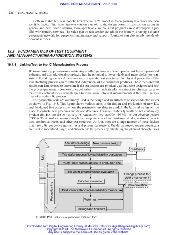
DC parametric tests are commonly used in the design and manufacture of semiconductor wafers
as shown in Fig. 19.3. This figure shows various steps in the design and production of new ICs,
and the dashed line boxes show how the parametric test data are used. In the lab, trial wafers will be
made to evaluate new processes and device structures. These test wafers typically do not contain any
product die, but consist exclusively of parametric test modules (PTMs) or test element groups
(TEGs). These wafers contain many basic components such as transistors, diodes, resistors, capaci-
tors, conductive traces, and other test structures. At first, there are a large number of these devices
that have different device geometries and process parameters. The dc parametric measurement data
are used to understand, target, and characterize the process by calculating the physical characteristics
New device design New process design
Feedback
Trial wafer-process/device/reliability evaluation
Lab
Transfer new process/device to production line
Trial wafer-process/device evaluation
Change process for
yield enhancement
Function evaluation Data correlation
Production line Production wafer-process/reliability monitor
Wafer test
Package and final test
FIGURE 19.3 What are dc parametric tests used for?
Downloaded from Digital Engineering Library @ McGraw-Hill (www.digitalengineeringlibrary.com)
Copyright © 2004 The McGraw-Hill Companies. All rights reserved.
Any use is subject to the Terms of Use as given at the website.