
Page 282 - Semiconductor Manufacturing Handbook
P. 282
Geng(SMH)_CH19.qxd 04/04/2005 20:00 Page 19.9
INSPECTION, MEASUREMENT, AND TEST
INSPECTION, MEASUREMENT, AND TEST 19.9
from the electrical data. Once the process has been developed to the point where its performance,
reliability, and yield targets have been achieved as verified by using parametric test data, the prod-
uct die can be added and the process can move into the pre-production phase. The PTM areas are
then significantly reduced or removed, with the product die taking their place. For a well-established
process in full production, it is frequently possible to eliminate the PTMs altogether and to have the
parametric test structures reside in the scribe lines between the die. The number of measurements is
also usually reduced since these impact the manufacturing time, but some dc parametric measure-
ments are still done to ensure that major process parameters are on track.
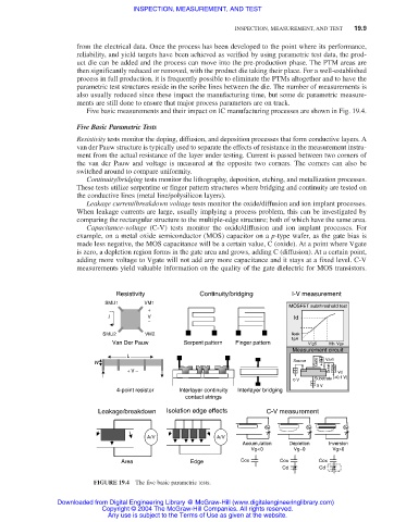
Five basic measurements and their impact on IC manufacturing processes are shown in Fig. 19.4.
Five Basic Parametric Tests
Resistivity tests monitor the doping, diffusion, and deposition processes that form conductive layers. A
van der Pauw structure is typically used to separate the effects of resistance in the measurement instru-
ment from the actual resistance of the layer under testing. Current is passed between two corners of
the van der Pauw and voltage is measured at the opposite two corners. The corners can also be
switched around to compare uniformity.
Continuity/bridging tests monitor the lithography, deposition, etching, and metallization processes.
These tests utilize serpentine or finger pattern structures where bridging and continuity are tested on
the conductive lines (metal line/polysilicon layers).
Leakage current/breakdown voltage tests monitor the oxide/diffusion and ion implant processes.
When leakage currents are large, usually implying a process problem, this can be investigated by
comparing the rectangular structure to the multiple-edge structure; both of which have the same area.
Capacitance-voltage (C-V) tests monitor the oxide/diffusion and ion implant processes. For
example, on a metal oxide semiconductor (MOS) capacitor on a p-type wafer, as the gate bias is
made less negative, the MOS capacitance will be a certain value, C (oxide). At a point where Vgate
is zero, a depletion region forms in the gate area and grows, adding C (diffusion). At a certain point,
adding more voltage to Vgate will not add any more capacitance and it stays at a fixed level. C-V
measurements yield valuable information on the quality of the gate dielectric for MOS transistors.
Resistivity Continuity/bridging I-V measurement
SMU1 VM1
MOSFET subthreshold test
+
I V Id
−
SMU2 VM2 Ileak
1pA
Van Der Pauw Serpent pattern Finger pattern V′gS Vth Vgs
Measurement circuit
L
Source Var1
W Gate
+ V − Drain A Vd
0 V Substrate (<0.1 V)
0 V
4-point resistor Interlayer continuity Interlayer bridging
contact strings
Leakage/breakdown Isolation edge effects C-V measurement
A/V A/V
Accumulation Depletion Inversion
Vg<0 Vg~0 Vg>0
Area Edge Cox Cox Cox
Cd Cd
FIGURE 19.4 The five basic parametric tests.
Downloaded from Digital Engineering Library @ McGraw-Hill (www.digitalengineeringlibrary.com)
Copyright © 2004 The McGraw-Hill Companies. All rights reserved.
Any use is subject to the Terms of Use as given at the website.