
Page 303 - Semiconductor Manufacturing Handbook
P. 303
Geng(SMH)_CH19.qxd 04/04/2005 20:00 Page 19.30
INSPECTION, MEASUREMENT, AND TEST
19.30 FINAL MANUFACTURING
Using orthogonal frequency division multiplexing (OFDM) as an example, these calculations are
made for each burst and data vector, resulting in an individual EVM (the error vector for a particu-
lar instant in time relative to the symbol clock).
Adjacent channel power. When two or more signals (f1 and f2) at different frequencies are
applied to an amplifier, nonlinearities in the amplifier cause the output to contain additional mixing
frequencies called intermodulation (IM) products. These occur at frequencies (mf1 ± nf2) and at
(mf2 ± nf1), where m + n is the order of the IM product. For example, the second order IM products
would be at f1 + f2, f1 − f2 and f2 − f1. Even-order products are located near the baseband, while
odd-order products are located on either side of the input signals. As an example, if two input tones
are applied to the input of the amplifier, the output consists of amplified versions of the two input
tones, plus odd-order intermodulation products caused by amplifier nonlinearity.
If the frequency spectrum is divided into channels of equal bandwidth located next to each other, and
the two input tones are applied, distortion in the amplifier causes signals to appear in the output adjacent
channels. In the digital-modulation world, the two tones at the input are really replaced by an infinite num-
ber of tones (or noise) within the defined channel bandwidth. The energy generated by amplifier nonlin-
earity in adjacent channels is called spectral regrowth and is measured as adjacent channel leakage.
The actual specifications take the measured spectral regrowth within a specified bandwidth and
ratio it as a relative quantity to the desired power in the main channel. This is done for each of the
two adjacent channels above and below the desired transmit channel, expressed in dB and is called
adjacent channel leakage ratio (ACLR).
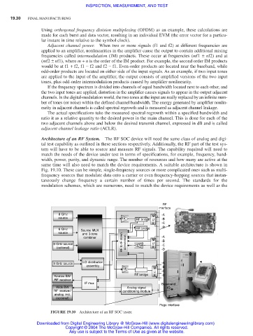
Architecture of an RF System. The RF SOC device will need the same class of analog and digi-
tal test capability as outlined in these sections respectively. Additionally, the RF part of the test sys-
tem will have to be able to source and measure RF signals. The capability required will need to
match the needs of the device under test in terms of specifications, for example, frequency, band-
width, power, purity, and dynamic range. The number of resources and how many are active at the
same time will also need to match the device requirements. A suitable architecture is shown in
Fig. 19.10. These can be simple, single-frequency sources or more complicated ones such as multi-
frequency sources that modulate data onto a carrier or even frequency-hopping sources that instan-
taneously change frequency a certain number of times per second. The standards for the
modulation schemes, which are numerous, need to match the device requirements as well as the
RF
interface
8 GHz -A
source PA RF bridge U M -B
X -C
-D
6 GHz Source MUX RF bridge
source
and 3-tone
combiner M -A
6 GHz source RF to IF down conversion LNA U -B
-C
(optional) X -D
LO distribution -A
8 GHz source
assembly -B
PA
PA M
U -C
RF bridge X -D
Narrow BW
RF receiver
IF mux Baseband
Wide BW Analog signal IQ
RF receiver/ conditioning module
analog inst.
(optional)
Pogo interface
FIGURE 19.10 Architecture of an RF SOC tester.
Downloaded from Digital Engineering Library @ McGraw-Hill (www.digitalengineeringlibrary.com)
Copyright © 2004 The McGraw-Hill Companies. All rights reserved.
Any use is subject to the Terms of Use as given at the website.