
Page 299 - Semiconductor Manufacturing Handbook
P. 299
Geng(SMH)_CH19.qxd 04/04/2005 20:00 Page 19.26
INSPECTION, MEASUREMENT, AND TEST
19.26 FINAL MANUFACTURING
Most system-on-chip (SOC) devices include PLL sections to generate appropriate clock signals
to be distributed to various functional blocks. An external oscillator may supply a basic clock signal
to the device and it may be multiplied or divided into suitable frequencies for each functional block.
In a serial data transmission SOC, an incoming receiver signal may contain its own clock that is
extracted by a PLL.
The power section is one of the most critical sections of the device that is frequently overlooked.
Optimum power supply, distribution, and bypass filtering are key to keeping noise and ripple to a
minimum to allow the device to function properly.
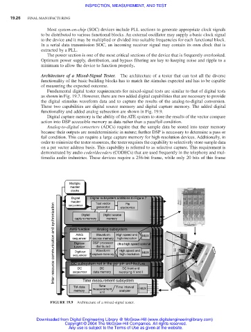
Architecture of a Mixed-Signal Tester. The architecture of a tester that can test all the diverse
functionality of the basic building blocks has to match the stimulus expected and has to be capable
of measuring the expected outcome.
Fundamental digital tester requirements for mixed-signal tests are similar to that of digital tests
as shown in Fig. 19.7. However, there are two added digital capabilities that are necessary to provide
the digital stimulus waveform data and to capture the results of the analog-to-digital conversion.
These two capabilities are digital source memory and digital capture memory. The added digital
functionality and added analog subsection are shown in Fig. 19.9.
Digital capture memory is the ability of the ATE system to store the results of the vector compare
action into DSP accessible memory as data rather than a pass/fail condition.
Analog-to-digital converters (ADCs) require that the sample data be stored into tester memory
because their outputs are nondeterministic in nature; further DSP is necessary to determine a pass or
fail condition. This can require a large capture memory for high-resolution devices. Additionally, in
order to minimize the tester resources, the tester requires the capability to selectively store sample data
on a per vector address basis. This capability is referred to as selective capture. This requirement is
demonstrated by audio coder/decoders (CODECs) that are used frequently in the telephony and mul-
timedia audio industries. These devices require a 256-bit frame, while only 20 bits of this frame
Multiple
master
clocks
Digital Digital subsystem additions to Figure 7
master Digital Test vector electronics
Inter resource communication and sychronization AWG function capture memory High speed and MUX
Pin
sequencer
generator
Digital source
capture memory
memory
Analog subsystem
Waveform
AWG
high resolution
sequencer
source memory
DSP processor
Digitizer
Ultra high speed optional
distributed
function
High speed and
Waveform
Digitizer
MUX
high resolution
sequencer
DC subsystem not in the per pin architecture
DC
DC front end
DC
data memory
sequencer
Time measurement subsystem
Time supplying V and I
TIA data measurement Time interval MUX
memory analyzer
unit
FIGURE 19.9 Architecture of a mixed-signal tester.
Downloaded from Digital Engineering Library @ McGraw-Hill (www.digitalengineeringlibrary.com)
Copyright © 2004 The McGraw-Hill Companies. All rights reserved.
Any use is subject to the Terms of Use as given at the website.